
SiC Substrate Resistivity: Conductive vs Semi-Insulating SiC
Introduction
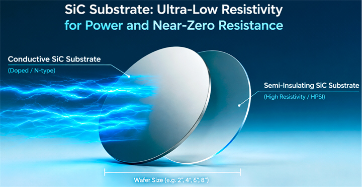
SiC substrate resistivity determines how the substrate interacts electrically with the device built on it. HMT, a SiC wafer manufacturer, supplies conductive 4H-N SiC substrates for current-carrying semiconductor structures and high-purity semi-insulating (HPSI) SiC substrates for RF, microwave and GaN-on-SiC applications. The important point is not whether a SiC wafer has “higher” or “lower” resistivity, but whether its electrical behavior matches the device architecture. Conductive and semi-insulating SiC therefore represent two different substrate strategies rather than two performance grades of the same product.
What Does SiC Substrate Resistivity Actually Tell You?
Resistivity describes how strongly a material opposes electrical current. For a SiC substrate, however, the value becomes meaningful only when it is considered together with the role that the substrate plays inside the finished semiconductor structure.
A substrate can function as part of an electrical path, or it can be expected to remain highly resistive so that the active device is electrically separated from the underlying material. This distinction is why two wafers made from the same 4H-SiC crystal system can be specified for very different semiconductor applications.
For practical wafer selection, resistivity should therefore be viewed as an architecture-related specification, rather than an isolated number.
Conductive SiC: When the Substrate Needs to Participate in Current Transport
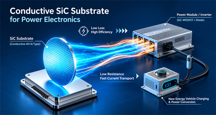
A conductive SiC substrate is designed to provide a relatively low-resistance electrical path through the semiconductor structure. This characteristic is particularly relevant to vertical power-device architectures, where electrical current travels through different layers of the device and substrate.
HMT's current conductive 4H-SiC product range includes 4-, 6- and 8-inch wafers, with a listed thickness of 350 µm and conductive N-type material.
The important engineering question is therefore not simply:
“Is this SiC wafer conductive?”
It is:
“Does the substrate provide the electrical behavior required by the intended device structure?”
That distinction makes resistivity a functional specification rather than just a material-property label.
Why Does Low Resistivity Matter in Vertical SiC Power Devices?
In a vertical power device, the substrate is not merely a mechanical support. It can form part of the vertical electrical structure through which current is transported.
A simplified structure can be represented as:
Metal Contact → Device Layers → SiC Substrate → Backside Contact
If the substrate introduces unnecessary electrical resistance, it can contribute to the overall resistance of the device. Reducing resistive contributions in the current path is therefore one consideration in designing efficient vertical power semiconductor structures.
This is also why conductive SiC substrates are commonly associated with power-device applications rather than RF isolation structures. Wolfspeed similarly categorizes conductive SiC substrates under its SiC materials for power electronics.
How Is Conductive SiC Resistivity Controlled?
The electrical behavior of a conductive SiC wafer is influenced by the crystal material, intentional doping, carrier concentration and manufacturing process.
For example, HMT's 4-inch conductive 4H-SiC specification identifies nitrogen as the dopant and lists a resistivity range of 0.015–0.028 Ω·cm for that product. The same product specification lists a 100 mm wafer diameter, 350 ± 25 µm thickness, micropipe density ≤0.5 ea/cm² and TTV ≤10 µm.
These numbers illustrate an important point: resistivity should be evaluated together with wafer geometry, defect density, thickness, surface condition and intended device process.
Semi-Insulating SiC: When the Substrate Should Stay Electrically Quiet
A semi-insulating SiC substrate serves a fundamentally different purpose.
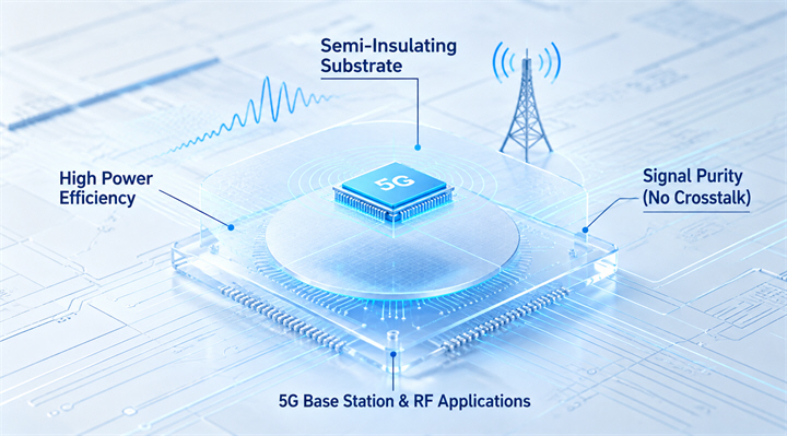
Instead of providing an efficient current path, the substrate is engineered to exhibit very high electrical resistivity. This helps isolate the active semiconductor structure from unwanted substrate conduction and is particularly relevant to high-frequency device architectures.
HMT describes its HPSI SiC substrates as platforms for RF devices, microwave electronics, GaN epitaxial growth and high-frequency communication systems.
Wolfspeed likewise separates its SiC material portfolio into conductive substrates for power electronics and semi-insulating substrates for GaN-on-SiC RF devices.
Why Does RF Use High-Resistivity SiC?
RF circuits operate with rapidly changing electrical signals. Unwanted conduction through the substrate can create additional electrical coupling and parasitic effects that are undesirable in high-frequency structures.
For this reason, the substrate in a GaN-on-SiC RF structure is generally expected to provide electrical isolation while simultaneously offering a strong thermal and mechanical foundation.
A simplified architecture is:
RF Device / GaN Epitaxy → HPSI SiC Substrate
The SiC does not need to serve as the primary vertical current path in the same way as a conductive substrate used in a power device. Instead, its combination of electrical isolation and thermal properties becomes particularly valuable.
Wolfspeed's HPSI product descriptions, for example, specify 4H-SiC HPSI substrates at ≥1E8 Ω·cm for certain production products and explicitly identifies them for RF material applications.
HPSI Is Not Simply “Higher-Resistance SiC”
This is one of the most important distinctions for wafer buyers.
It would be misleading to treat HPSI SiC as simply a conductive SiC wafer with its resistivity pushed higher. The two material categories are intended for different electrical roles and may be manufactured and qualified around different device requirements.
HMT's 6-inch HPSI product, for example, is specified as 150 ± 0.2 mm diameter, 500 ± 25 µm thickness and HPSI material, with the page describing applications including 5G, radar, aerospace and RF power devices.
Therefore, a buyer should begin with the device architecture and application, then determine the appropriate resistivity class.
Does Higher SiC Resistivity Mean a Better Wafer?
No. Higher resistivity does not automatically mean better SiC.
A high-resistivity substrate can be desirable for one device architecture and inappropriate for another. If the substrate is expected to participate in current transport, excessive electrical isolation would not serve the same purpose as it does in an RF substrate.
The correct specification is therefore application-dependent.
For example, HMT's conductive 4H-SiC product is positioned for conductive applications, while its HPSI products are positioned for RF and GaN-on-SiC structures.
The more useful question is: What electrical role will the SiC substrate play after device fabrication?
HMT SiC Wafer Manufacturer: Conductive and HPSI Substrate Options
HMT's SiC substrate portfolio covers both electrical categories, allowing customers to select material according to the intended semiconductor architecture rather than forcing different applications into a single wafer type.
For conductive applications, HMT lists 4H-SiC N-type wafers in 4-, 6- and 8-inch formats, while its 4-inch product page provides detailed specifications including nitrogen doping and a 0.015–0.028 Ω·cm resistivity range.
For high-frequency applications, HMT offers HPSI SiC substrates in larger wafer formats. Its 6-inch HPSI page specifies 150 ± 0.2 mm diameter and 500 ± 25 µm thickness, while the HPSI RF page describes applications including RF, microwave and GaN-on-SiC technologies.
For customers comparing available substrate configurations, see HMT's 4H-SiC Wafer Manufacturer
page for conductive material options and specifications.
For RF and GaN-on-SiC requirements, see HMT's HPSI SiC Wafer for RF and GaN-on-SiC
.
For a specific 4-inch conductive substrate specification, see the 4-inch 4H-SiC Wafer
page.
For larger HPSI requirements, see the 6-inch 4H-HPSI SiC Wafer
FAQWhat is SiC substrate resistivity?
SiC substrate resistivity describes the material's resistance to electrical current flow. In semiconductor applications, its importance depends on whether the substrate is intended to participate in current transport or provide electrical isolation.
What is the difference between conductive SiC and HPSI SiC?
Conductive SiC is designed to provide an electrically conductive substrate, while HPSI SiC is engineered for very high electrical resistivity. Conductive SiC is commonly associated with power-device structures, whereas HPSI SiC is widely used for RF and GaN-on-SiC applications.
Is lower SiC resistivity always better?
No. Lower resistivity is useful when the substrate needs to support electrical current, but it is not the objective for a substrate whose role includes electrical isolation.
 E-mail: kim@homray-material.com;tina@homray-material.com
HMT Silicon Carbide (SiC) Wafer Website: www.sicwafer-hmt.com