
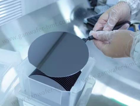
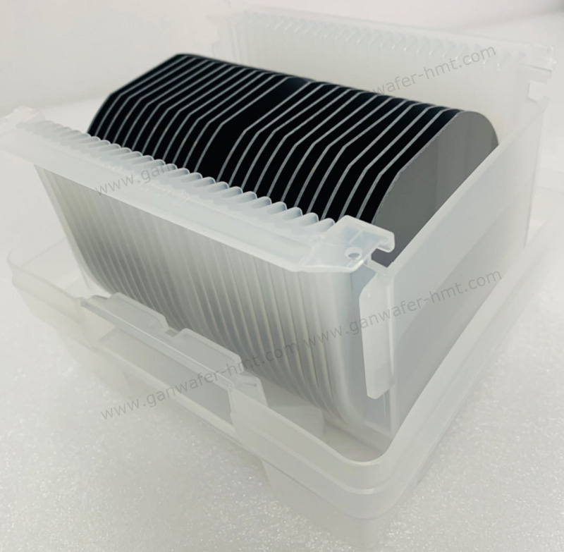
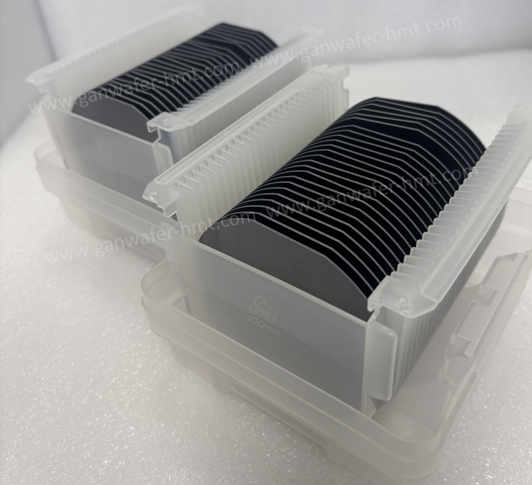
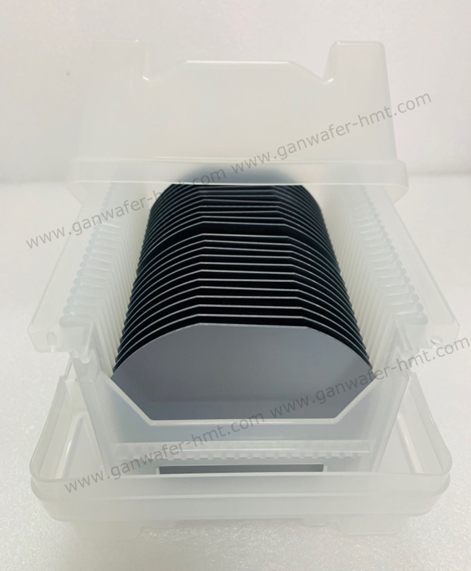
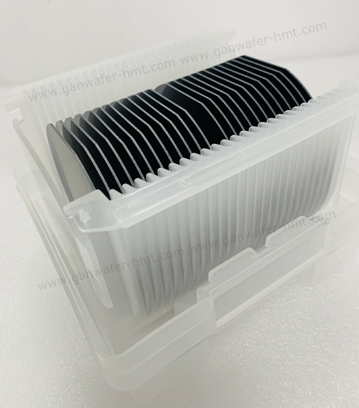
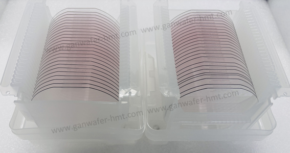
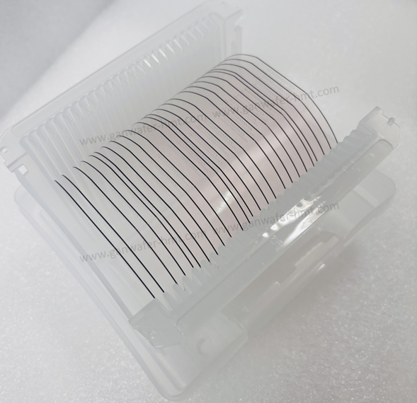
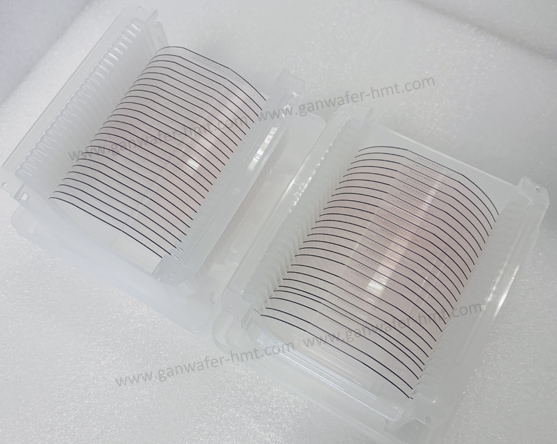
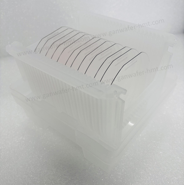
2 Inch GaN-on-Si Epi Wafer AlGaN/GaN Power HEMT
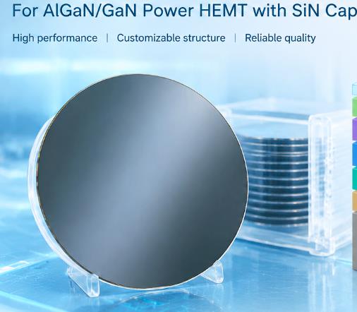
GaN-On-Si Epi Wafer For Power HEMT
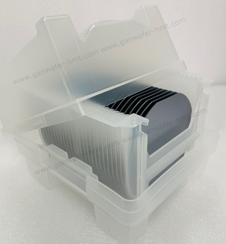
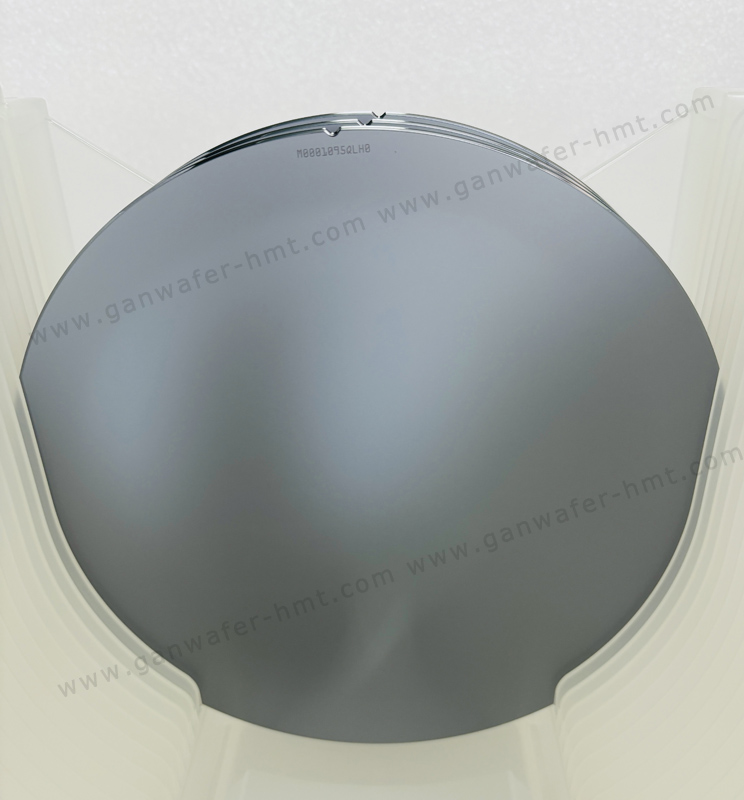
Substrate Diameter:2 inch (111)
Substrate Thickness:675um
Cap Layer: SiN Cap
Product Description
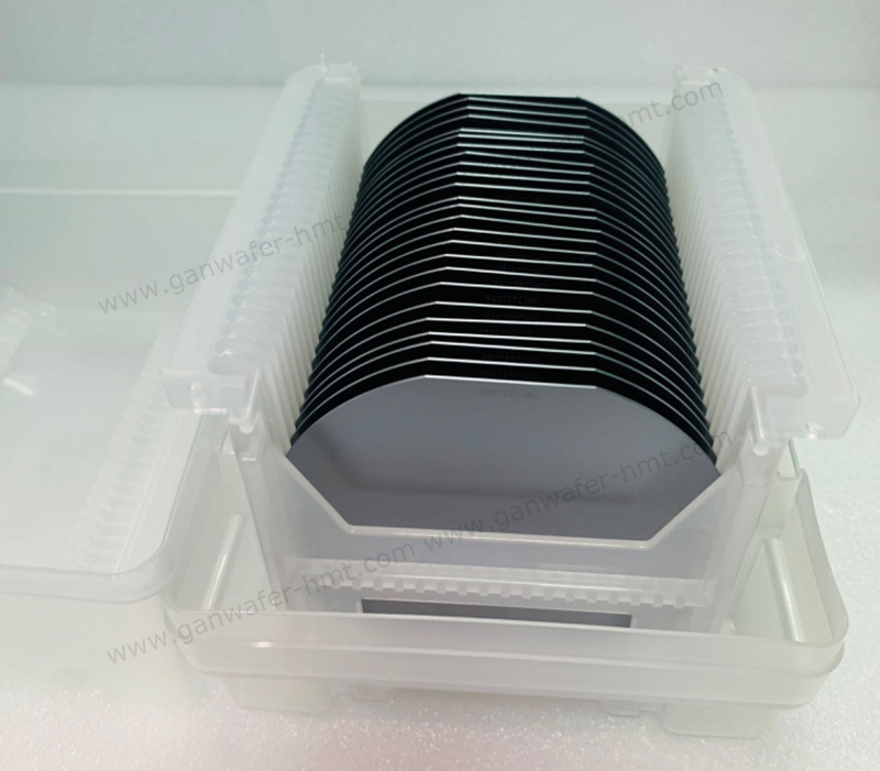
2 Inch GaN-on-Si Epi Wafer for Power HEMT Applications
Homray is an experienced GaN epitaxial wafer manufacturer providing customized GaN epi solutions for Power and RF semiconductor applications. Homray Material Technology provides 2 inch GaN-on-Si epi wafers with AlGaN/GaN heterostructure and optional SiN cap layers for Power HEMT device development. These GaN epitaxial wafers are designed for researchers, semiconductor companies, and device manufacturers requiring high-quality GaN layers on silicon substrates for high-efficiency power switching applications.
GaN-on-Si technology combines the superior electrical properties of gallium nitride with the cost advantages and mature manufacturing ecosystem of silicon substrates. The AlGaN/GaN heterostructure enables high electron mobility and supports the fabrication of advanced normally-off and normally-on GaN HEMT devices. The AlGaN/GaN heterostructure enables high electron mobility and forms a two-dimensional electron gas (2DEG) channel, which is the fundamental operating principle of GaN HEMT technology.
What Is a 2 Inch GaN-on-Si Epi Wafer?
A 2 inch GaN-on-Si epi wafer is a semiconductor substrate consisting of epitaxially grown GaN layers deposited on a silicon wafer, typically using MOCVD technology.
The standard structure includes a silicon (111) substrate, buffer layers, GaN channel layer, AlGaN barrier layer, and optional GaN or SiN cap layer. The AlGaN/GaN interface creates a two-dimensional electron gas (2DEG) channel, which is essential for high-performance HEMT devices.
For Power HEMT applications, the epitaxial structure can be customized according to breakdown voltage, threshold voltage, and device architecture requirements. Commercial GaN-on-Si Power HEMT wafers commonly use AlGaN/GaN heterostructures with customized barrier and cap designs.
GaN power semiconductor technology has attracted significant attention due to its high switching frequency, high efficiency, and compact device design.
AlGaN/GaN Heterostructure for High Efficiency Power Devices
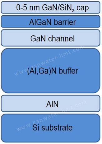 The AlGaN/GaN structure is the key functional layer of GaN HEMT devices.
Compared with conventional silicon-based power devices, GaN offers a wider bandgap of approximately 3.4 eV and a higher critical electric field, enabling higher switching frequency, lower conduction loss, and improved power density.
The AlGaN barrier layer generates a high-density 2DEG channel at the AlGaN/GaN interface, allowing Power HEMTs to achieve low on-resistance and fast switching characteristics.
Homray can provide customized AlGaN barrier thickness, GaN channel thickness, buffer design, and electrical characteristics based on customer device requirements. For higher voltage switching requirements, customers can also explore our GaN-on-Si Epi Wafer for Power HEMT platform.
SiN Cap Layer for GaN HEMT Device Protection
The SiN cap layer is an important component for improving GaN HEMT device reliability.
A SiN cap or passivation layer can help protect the AlGaN surface, reduce surface-related trapping effects, and improve device stability during high-voltage switching operation.
Homray offers GaN-on-Si epi wafers with optional SiN cap structures for customers developing Power HEMT devices, including customized SiN thickness and epi layer combinations.
Standard Specification of 2 Inch GaN-on-Si Epi Wafer
| Parameter | Specification |
|---|---|
| Substrate | Silicon (111) |
| Wafer Diameter | 2 inch |
| Epitaxial Structure | AlGaN/GaN Heterostructure |
| Application | Power HEMT |
| Cap Layer | SiN / GaN Cap Optional |
| Growth Method | MOCVD |
| Structure Type | D-mode / E-mode Customizable |
| Buffer Design | Customized |
| Surface | Epi-ready |
Advantages of Homray GaN-on-Si Epi Wafer
Customized Epitaxial Design
Homray supports customized GaN epi structures including AlGaN barrier engineering, GaN channel optimization, buffer layer design, and SiN cap integration.
Suitable for Research and Pilot Production
The 2 inch format provides flexibility for university research, prototype development, and early-stage GaN HEMT device fabrication before moving to larger wafer platforms.
High Compatibility with GaN Power Electronics
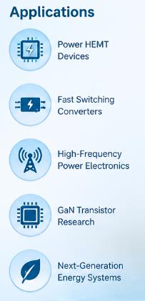
GaN-on-Si epi wafers are suitable for applications including:
- Power HEMT devices
- Fast switching converters
- High-frequency power electronics
- GaN transistor research
- Next-generation energy systems
Besides power switching devices, GaN-on-Si technology is also widely used for RF HEMT applications.
FAQ
What is a 2 inch GaN-on-Si epi wafer?
A 2 inch GaN-on-Si epi wafer is a silicon substrate with epitaxially grown GaN layers designed for semiconductor devices such as AlGaN/GaN HEMTs.
Why use AlGaN/GaN structure for Power HEMT?
The AlGaN/GaN heterostructure creates a high-density 2DEG channel, providing high electron mobility, low resistance, and fast switching capability for power devices.
Can Homray provide SiN cap GaN-on-Si epi wafers?
Yes. Homray provides customized GaN-on-Si epi wafers with optional SiN cap layers for Power HEMT device fabrication and reliability improvement.
Related Products
 E-mail: kim@homray-material.com;tina@homray-material.com
HMT Silicon Carbide (SiC) Wafer Website: www.sicwafer-hmt.com