
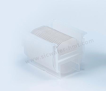
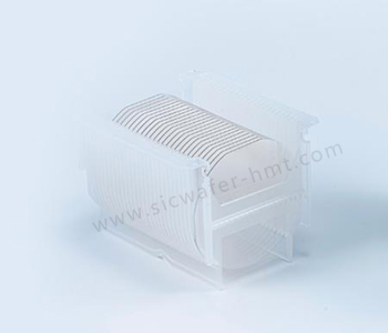
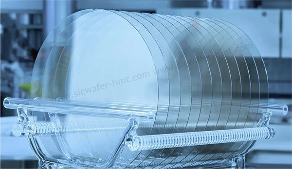
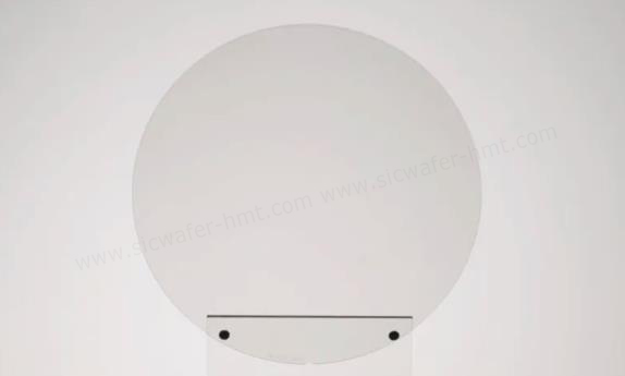
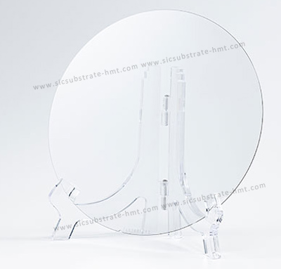
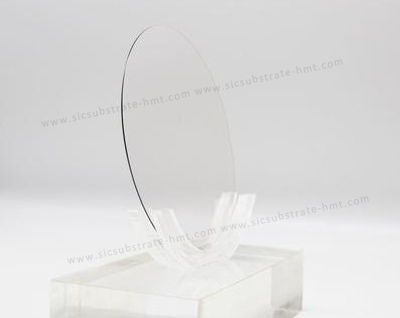
6 Inch 4H-HPSI SiC Wafer – P Grade
Diameter:150±0.2mm
Grade: P
Thickness: 500±25um
Type: HPSI
Product Description
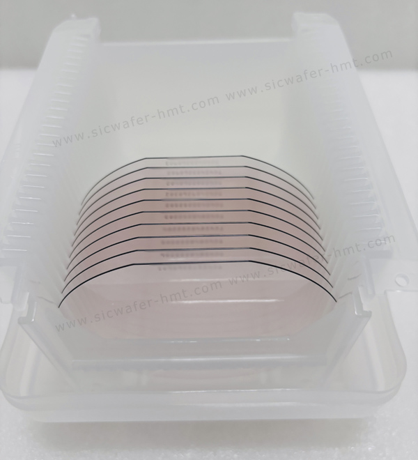
As a premier 4H-SiC wafer manufacturer, Homray offers 6 inch high-purity semi-insulating (HPSI) silicon carbide substrates that serve as the industry-standard foundation for high-performance RF devices and GaN-on-SiC epitaxy. Our P-grade wafers are engineered specifically for demanding 5G infrastructure, radar systems, and aerospace applications.
Product Overview
Our HPSI 4H-SiC wafers feature exceptional resistivity (≥1E7 Ω·cm) and ultra‑low micropipe density (< 0.5 cm⁻²), ensuring superior electrical insulation and minimal defects. This translates directly into higher device yields and better thermal management for HEMTs and MMICs. The precise diameter (150 ± 0.2 mm) and thickness (500 ± 25 µm) guarantee compatibility with standard semiconductor fabrication lines.
Key Applications
- 5G Communications – Base stations, massive MIMO, and core network hardware
- Defense & Aerospace – Radar, electronic warfare (EW), and satellite transceivers
- RF Power Devices – High-electron-mobility transistors (HEMTs) and monolithic microwave integrated circuits (MMICs)
- Optoelectronics – High-power LEDs and laser diodes
Technical Specifications (6″ P‑Grade)
| Diameter | 150 ± 0.2 mm |
| Thickness | 500 ± 25 µm |
| Resistivity | ≥ 1E9 Ω·cm (semi‑insulating) |
| Micropipe Density | < 0.2 cm⁻² |
| Surface Roughness | < 0.2 nm (epi‑ready) |
| Grade | P (Production) |
Why Choose Homray?
- In‑house growth – Full control over crystal quality and supply chain
- Customization – Available in 4″, 6″, and 8″ with tailored specifications
- Quality assurance – 100% inspection with advanced metrology tools
- Global shipping – Fast delivery to leading semiconductor fabs worldwide
Frequently Asked Questions
What is the difference between HPSI and N‑type SiC wafers?
What is the minimum order quantity (MOQ)?
Related Products
 E-mail: kim@homray-material.com;tina@homray-material.com
HMT Silicon Carbide (SiC) Wafer Website: www.sicwafer-hmt.com