
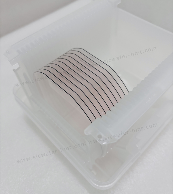
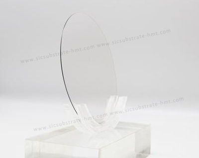
Un-doped Semi-insulating SiC Substrate Suppliers
Diameter: 100/150/200mm
Grade: D/R/P
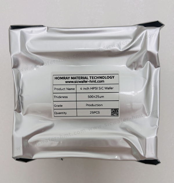
Thickness: 500±25um
Type: HPSI
Product Description
WHO WE ARE
Trusted Un-doped Semi-insulating SiC Substrate Suppliers – Powering the Global RF Revolution
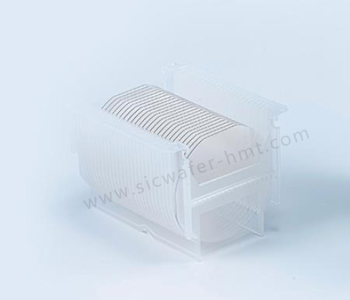
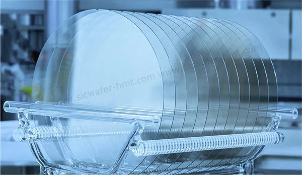
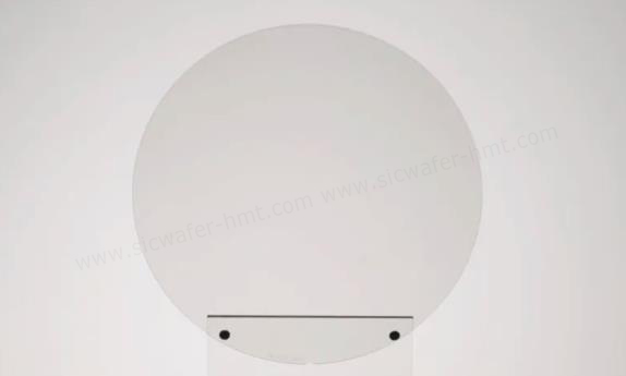
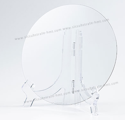
As a premier supplier of un-doped semi-insulating SiC substrates, HMT delivers best 4H-SiC wafers manufactured via advanced Physical Vapor Transport (PVT) technology. Our high-purity semi-insulating (HPSI) substrates feature exceptional electrical resistivity (≥1×10¹⁰ Ω·cm) and ultra-low micropipe density (≤0.2 cm⁻²). Available in 4 inch (100mm), 6 inch (150mm), and 8 inch (200mm) diameters, our wafers are the preferred foundation for GaN heteroepitaxy, delivering the optimal combination of high thermal conductivity (~4.9 W/cm-K) and wide bandgap (3.23 eV) required for high-power RF devices.
Our substrates are fully differentiated from conductive SiC products used in automotive EV applications. They are purpose-built for communications infrastructure, phased-array radar, and satellite payloads – markets that demand uncompromising signal integrity and thermal management.
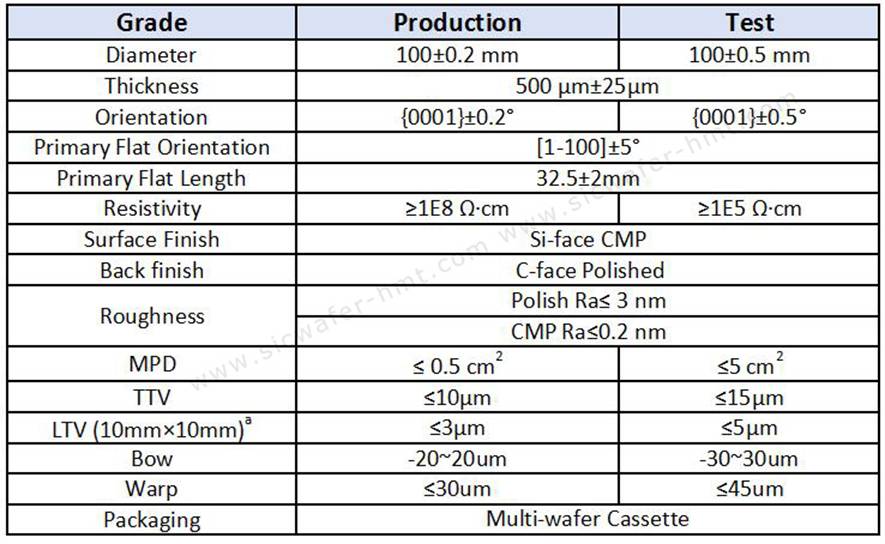
CORE TECHNICAL SPECIFICATIONS
Precision Engineered for High-Frequency Performance
We offer highly competitive pricing across all grades and diameters, with significant volume discounts for bulk orders. Our mass production capabilities ensure stable supply chain and short lead times. Whether you are procuring for R&D prototyping or high-volume production, our flexible ordering options—from small-batch research quantities to large-scale production shipments—are designed to accommodate your project timeline and budget. Contact our sales team today for a customized quote based on your specific diameter, grade, thickness, and quantity requirements. We are committed to providing the best price-to-performance ratio in the market for high-quality semi-insulating SiC substrates.
TECHNOLOGY TRENDS & FUTURE ROADMAP
GaN-on-SiC: The Industry Standard, Evolving Further
GaN-on-SiC remains the dominant heteroepitaxial solution for RF power amplifiers. However, the industry is rapidly moving toward next-generation integration:
-
Advanced Thermal Dissipation: Integrating SiC with aluminum nitride (AlN) nucleation layers and diamond heat-spreading layers to further lower junction temperatures and boost device reliability.
-
Multi-functional Integrated RF Chips: Development of single-chip solutions that combine signal amplification with filtering functions, simplifying base station and radar module architectures and reducing assembly costs for downstream OEMs.
These innovations ensure that un-doped semi-insulating SiC substrates will remain at the forefront of RF semiconductor materials for the next decade.
Related Products

 E-mail: kim@homray-material.com;tina@homray-material.com
HMT Silicon Carbide (SiC) Wafer Website: www.sicwafer-hmt.com