
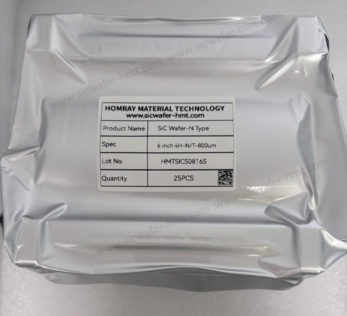
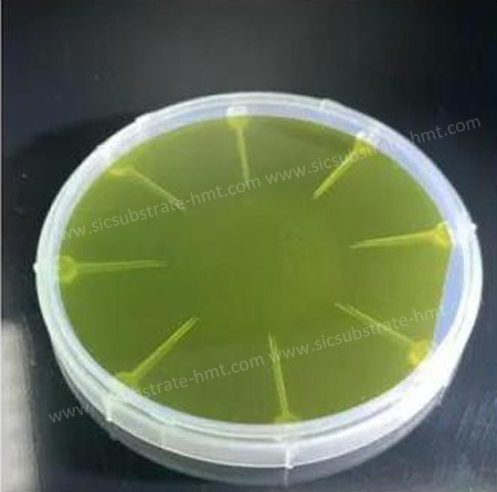
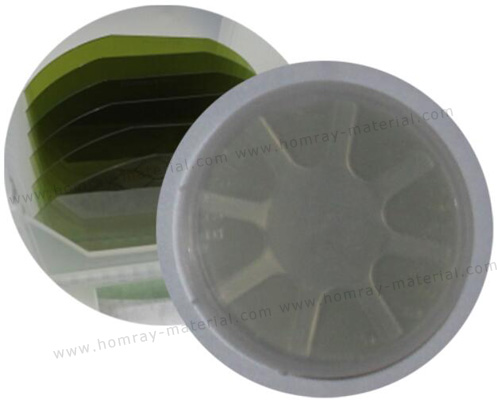
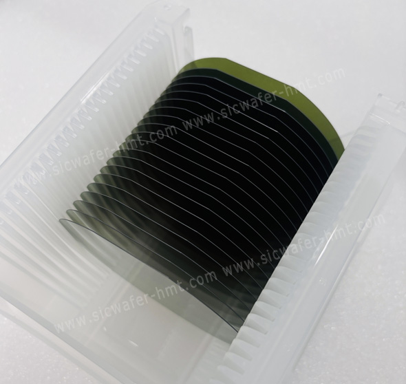
Customizing 6'' SiC Wafer N Type Supplier
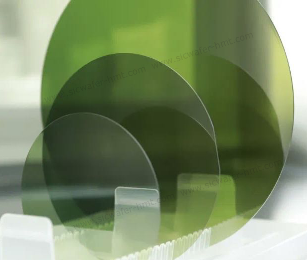
Diameter: 150±0.2mm
Grade: Production
Thickness: 350um/500um/800um
Type: Conductive N
Product Description
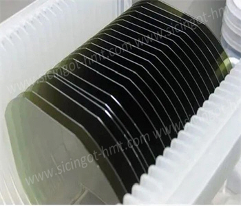
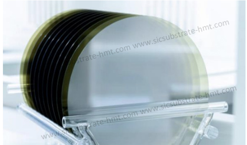
Supporting innovation at every level, HMT as a specialized SiC Wafer Manufacturer includes supplying customized 2''~8'' SiC Wafers. While we produce standard 350um 6 inch substrates, we maintain a unique capability to provide Non-standard customized SiC Wafer thickness 500um and 800um, which are crucial for research, prototyping, and specific optoelectronic applications. Contact us for all your SiC substrate needs.
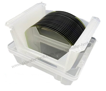
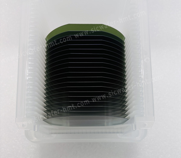
Non-standard customized SiC Wafer Spec
- Poly type: 4H
- Orientation: 4° toward <11-20> ± 0.5°
- Dopant: Nitrogen
- Diameter: 150±0.25mm
- Thickness: 500um/800um Customization
- Resistivity: 0.015-0.025ohm.cm
- Grade: D/R/P
- TTV/BOW: ≤10um/ -35~35um

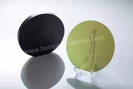
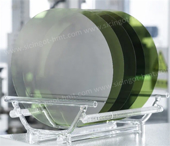
Conductive SiC Substrate Wafer (n-type): In the Physical Vapor Transport (PVT) method, the purity of the SiC source powder significantly influences the quality of the wafers. The powder typically contains trace amounts of impurities such as nitrogen (N), boron (B), aluminum (Al), and iron (Fe). Among these, nitrogen acts as an n-type dopant, introducing free electrons into silicon carbide, while boron and aluminum serve as p-type dopants, generating free holes. To produce n-type conductive SiC wafers, nitrogen gas is introduced during the crystal growth process. This compensates for the holes generated by boron and aluminum, while the remaining free electrons render the SiC electrically n-type.
Conductive SiC Wafer: Unlike traditional silicon-based power device fabrication processes, SiC power devices cannot be manufactured directly on bare SiC substrates. Instead, a silicon carbide epitaxial layer must be grown on a conductive substrate to form a SiC epitaxial wafer, which is then used to produce power devices.
These are suitable for high-temperature and high-voltage environments and are widely used in applications such as new energy vehicles, photovoltaics, smart grids, and rail transportation.
Related Products
![]() E-mail: kim@homray-material.com;tina@homray-material.com
E-mail: kim@homray-material.com;tina@homray-material.com
HMT Silicon Carbide (SiC) Wafer Website: www.sicwafer-hmt.com