

2''(50.8mm) 4H-SiC Wafer Supplier
Diameter: 50.8±0.38mm
Grade: Production
Thickness: 330±25um
Type: Conductive N
Product Description
2 Inch 4H-SiC Wafer Manufacturer | 50.8 mm Conductive N-Type SiC Substrate
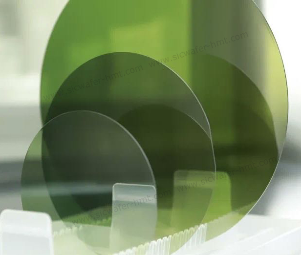
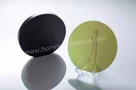
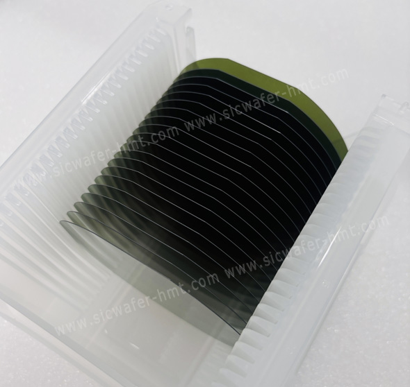
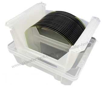
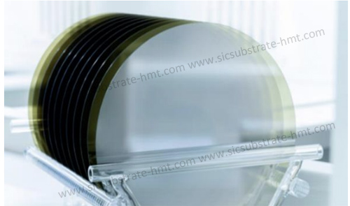
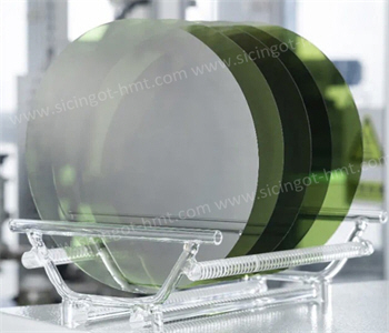
HMT provides 2 inch (50.8 mm) 4H-SiC wafers for semiconductor research, prototype development and specialty device fabrication. These small-diameter silicon carbide substrates are designed for customers who require a compact wafer format for material evaluation, process development or laboratory-scale device manufacturing.
The 2 inch SiC wafer is available in conductive N-type 4H-SiC with a production-grade specification. Compared with larger wafer formats, the 50.8 mm platform offers a practical option for research programs, pilot processes and applications where wafer size, material availability and development cost need to be carefully balanced.
2 Inch 4H-SiC Wafer Specifications
| Parameter | Specification |
| Material | Silicon Carbide (SiC) |
| Polytype | 4H |
| Diameter | 50.8 ± 0.38 mm |
| Wafer Size | 2 INCH |
| Conductivity | Conductive N-type |
| Grade | Production |
| Standard Thickness | 350 ± 25 μm |
| Surface | Polished |
| Customization | Diameter, thickness, surface specifications can be discussed |
| Resistivity | 0.015-0.028ohm.cm |
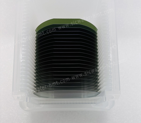
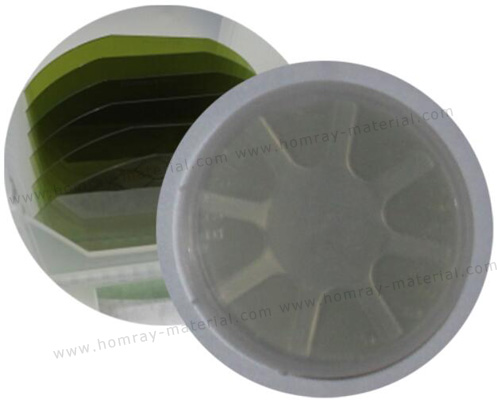
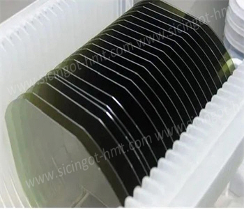
| Packaging | Semiconductor wafer cassette |
Why Choose a 2 Inch SiC Wafer?
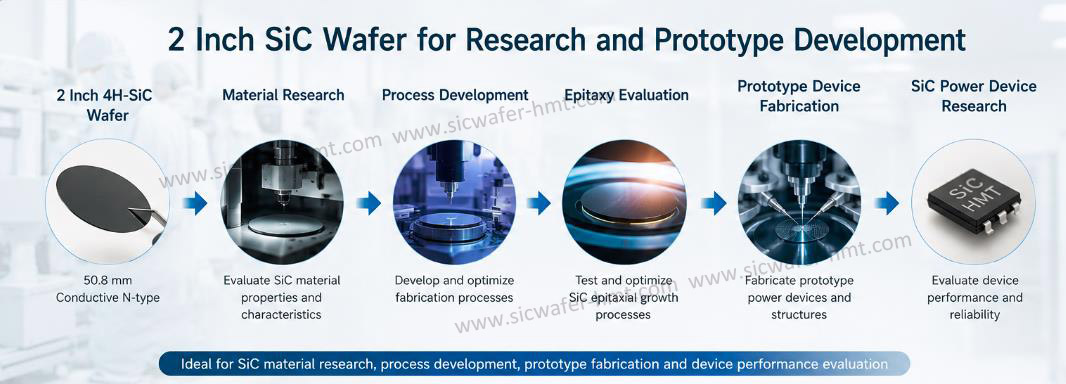
 A 2 inch SiC substrate is particularly useful when a development project does not require a large-area wafer. The 50.8 mm format allows research teams and process engineers to evaluate SiC material, develop fabrication parameters and validate device concepts before moving to larger wafer sizes.
The compact wafer format can also simplify material consumption during early-stage development. For customers working on specialized SiC processes, a 2 inch substrate can provide a practical platform for process qualification, laboratory testing and prototype device fabrication.
For customers moving from laboratory-scale development to larger wafer formats, our 4 inch 4H-SiC wafers provide a larger substrate platform for production-oriented semiconductor processes.
4H-SiC Substrate for Research and Prototype Development
The 4H-SiC crystal structure is widely used as a substrate material for silicon carbide semiconductor development. Its electrical, thermal and mechanical characteristics make it suitable for research involving wide-bandgap semiconductor devices.
HMT's 2 inch 4H-SiC wafers can be considered for:
* SiC material research
* Semiconductor process development
* Prototype power device fabrication
* SiC epitaxial process evaluation
* MOSFET and Schottky diode research
* Device structure verification
* University and laboratory semiconductor projects
* Specialty SiC component development

2 Inch SiC Wafer Supplier for Global Semiconductor Projects
HMT supports SiC material supply for customers involved in semiconductor research, process development and prototype manufacturing. In addition to 2 inch 4H-SiC wafers, our SiC product portfolio covers different wafer diameters, material grades and substrate configurations.
If you are evaluating a 2 inch SiC wafer for a new semiconductor process, please provide your required diameter, thickness, conductivity type, orientation and surface condition. HMT can review the specifications and provide a suitable wafer solution for your project.
Frequently Asked Questions
What is the diameter of a 2 inch SiC wafer?
A standard 2 inch SiC wafer has a nominal diameter of 50.8 mm. HMT currently offers 2 inch 4H-SiC wafers with a diameter specification of 50.8 ± 0.38 mm.
What type of SiC is available for the 2 inch wafer?
The standard product is conductive N-type 4H-SiC. Other specifications can be discussed according to the requirements of the semiconductor process.
Choosing the Right SiC Wafer Size
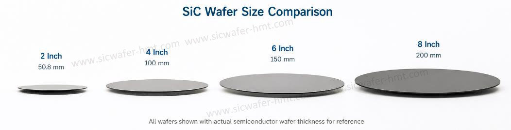
2 inch SiC wafer: suitable for laboratory research, process development and prototype fabrication.
4 inch SiC wafer: suitable for expanded process evaluation and pilot semiconductor manufacturing.
6 inch SiC wafer: designed for larger-area semiconductor development and production-oriented applications.
8 inch SiC wafer: intended for advanced large-diameter SiC semiconductor manufacturing.
Related Products

 E-mail: kim@homray-material.com;tina@homray-material.com
HMT Silicon Carbide (SiC) Wafer Website: www.sicwafer-hmt.com