
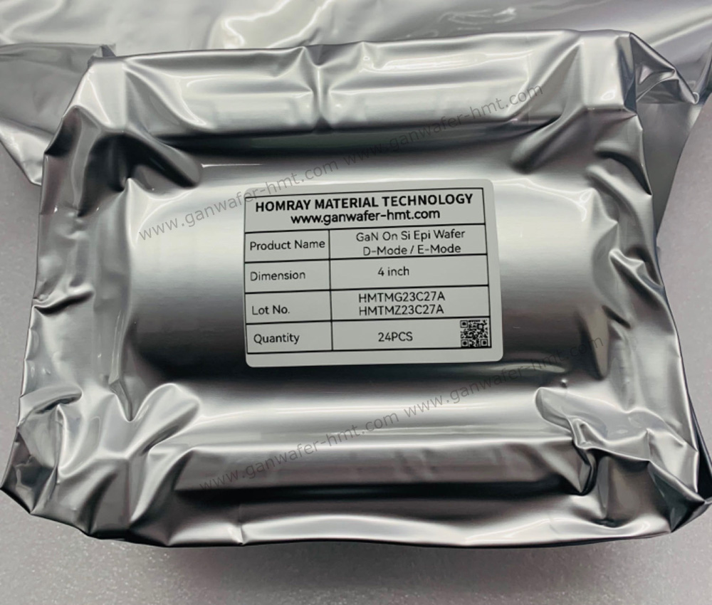
GaN On Si Epi Wafer
Project Description
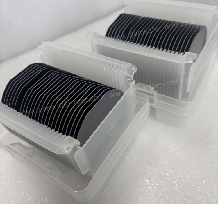
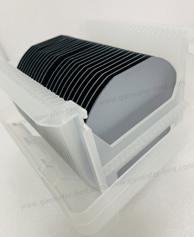
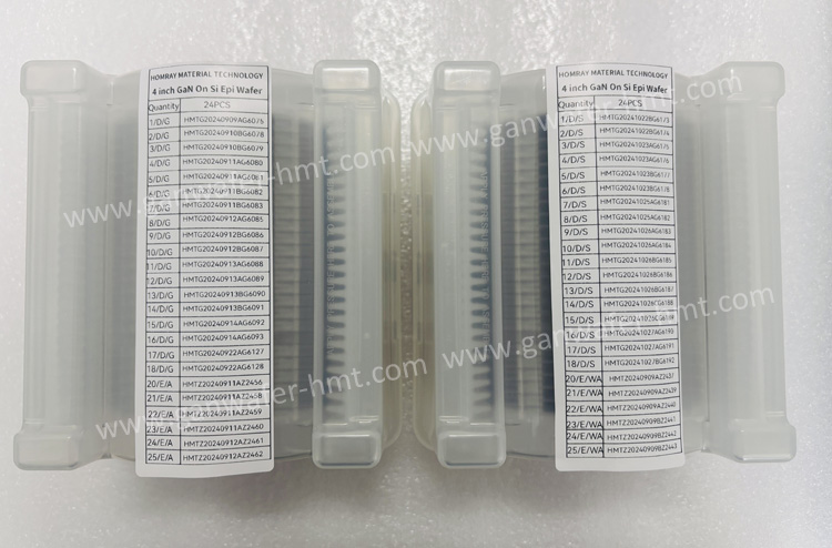
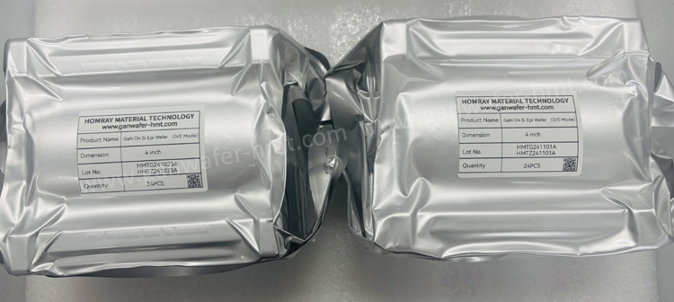
As a trusted GaN Epi Wafer Supplier, we manufacture 4inch 6inch and 8inch GaN On Si Epi Wafer, include D-Mode & E-Mode structure. The cap layer of D-Mode is GaN Cap or SiN Cap (Thickness 0-5nm), E-Mode is p-GaN Cap which doped with Mg (Thickness 90-100nm). You can customize your epi layer thickness based on your project requirements. Get a quote today!
![]() E-mail: kim@homray-material.com;tina@homray-material.com
E-mail: kim@homray-material.com;tina@homray-material.com
HMT Silicon Carbide (SiC) Wafer Website: www.sicwafer-hmt.com