
Founded in 2009, HMT is the reliable manufacturer and producer of SiC Wafer & HEMT GaN Epi Wafer & Pure GaN Wafer. Our core products include Silicon Carbide (SiC) Substrate Wafer (4H-N, 4H-SI, 4H-P), SiC Epi Wafer (N-Type and P-Type Epi Layer), and high-performance GaN-On-SiC Epi Wafer / GaN-On-Si Epi Wafer and GaN Wafer . Homray is dedicated to producing high-quality Wafers for the wide bandgap semiconductor industry. As a leading supplier of SiC Wafer and GaN Epi Wafer , the company has built a global network of dealers and partners across Europe, the United States, Southeast Asia, and South America. In 2023, HMT achieved worldwide sales exceeding USD 82 million.
Widely recognized for its superior properties such as a wide bandgap, Silicon Carbide is considered the most promising compound semiconductor material for next-generation electronic devices. Thanks to its high critical electric field, SiC-based devices and modules enable both low energy losses and high-speed switching/oscillation performance. The addition of our GaN-on-SiC and GaN-on-Si epi wafers extends this technological leadership, catering to the growing demands of high-frequency and high-power applications, particularly in HEMT RF and power electronics.
HMT Products Range Include:
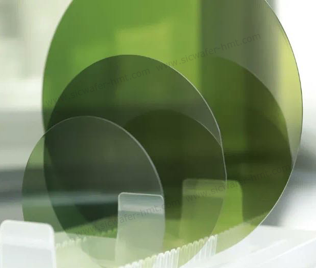
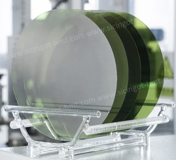
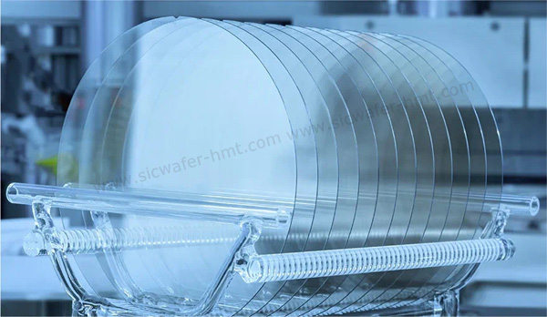
1.SiC Wafer / As-cut SiC Wafer(Unpolished) / SiC Boules / SiC Epi Wafer
- 2 inch(50.8mm) SiC Wafer (4H-N)
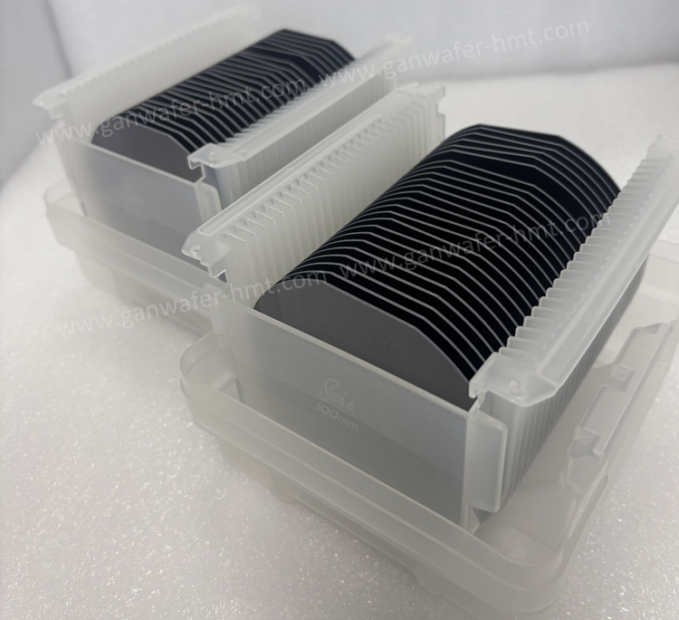
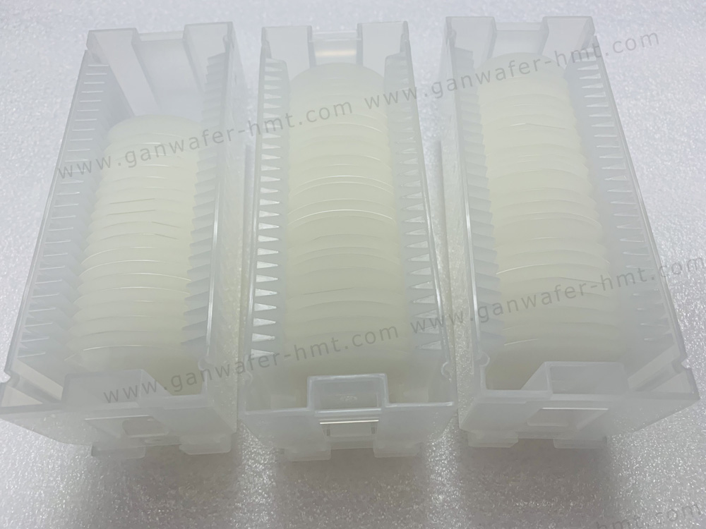
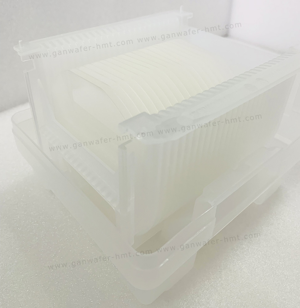
- 4 inch(100mm) 4H-N,4H-HPSI Grade SiC Substrate
- 6 inch(150mm) and 8 inch(200mm) SiC Wafers (4H-N,4H-SI, HPSI Optics)
- Thickness: 350um, 500um, support customized 700um 800um
- Grade: Dummy, Research, Production,Optics
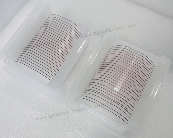
2. GaN Epi Wafer (Support Customized Epi Layer)
- GaN on SiC Epi Wafer (4inch,6inch,8inch)
- GaN on Si Epi Wafer (4inch,6inch,8inch)
- Structure: D-Mode, E-Mode, RF
- Cap Layer: GaN Cap, SiN Cap, pGaN Cap
3. GaN Substrate ( Un-doped, Si-doped, Fe-doped)
- GaN on Sapphire Wafer (GaN Thickness 4.5um)
- Pure GaN Wafer (GaN Thickness 400um,450um)
- Dimension: 2inch, 4inch, 6inch
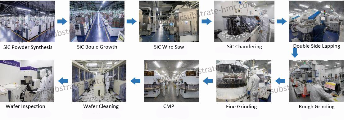
HMT SiC Wafer Processing
![]() E-mail: kim@homray-material.com;tina@homray-material.com
E-mail: kim@homray-material.com;tina@homray-material.com
HMT Silicon Carbide (SiC) Wafer Website: www.sicwafer-hmt.com