
Pure GaN Wafer
Project Description
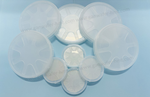
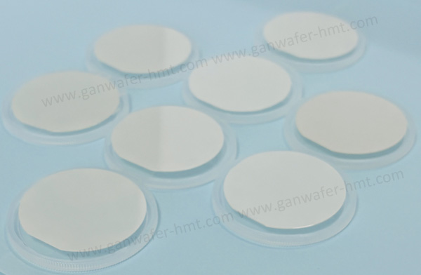
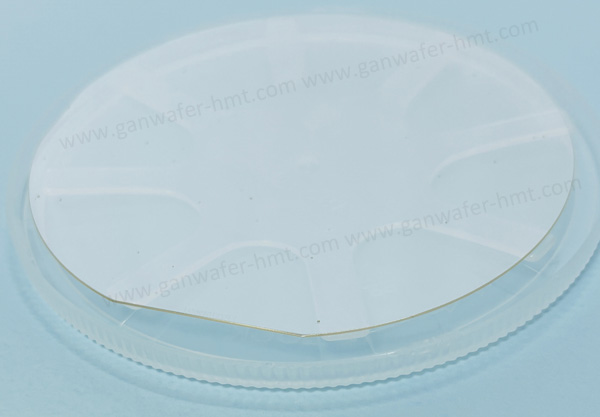
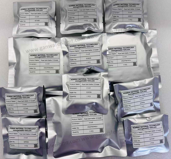
As a leading GaN Wafer Manufacturer, we produce Pure GaN Wafer, also called free-standing GaN Wafer with best price on the market. We have standard 2 inch Si-doped N type and 4 inch Un-doped/ Si-doped N type GaN Substrate. The GaN thickness is 400um/450um. we also have larges size 6 inch and 8 inch GaN Substrate now. If you are interested in our GaN products, please feel free to contact us.
![]() E-mail: kim@homray-material.com;tina@homray-material.com
E-mail: kim@homray-material.com;tina@homray-material.com
HMT Silicon Carbide (SiC) Wafer Website: www.sicwafer-hmt.com