
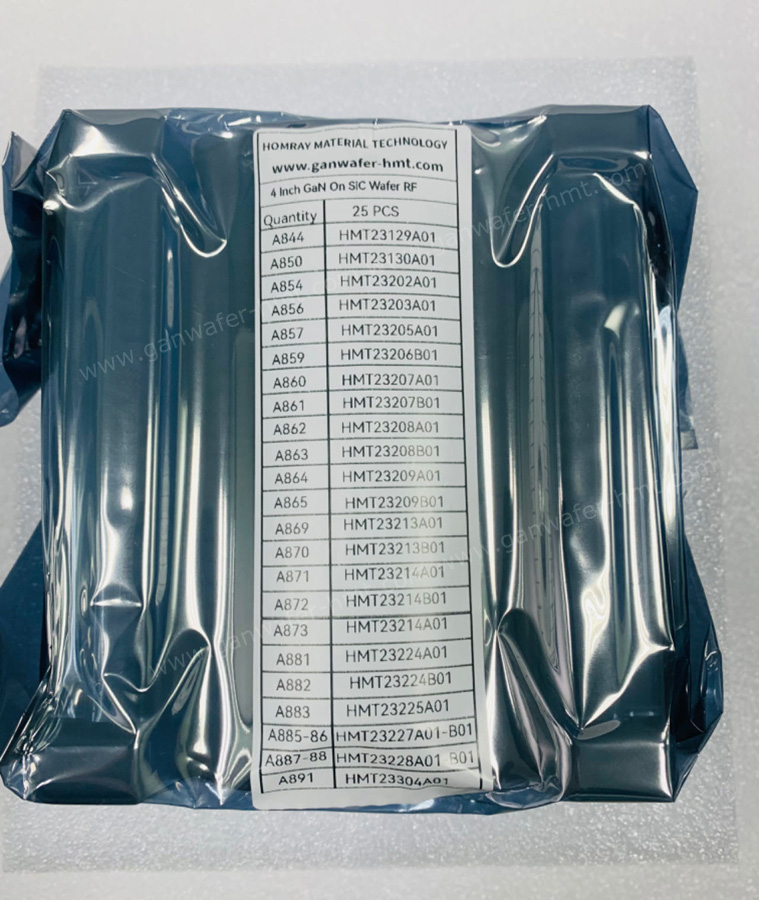
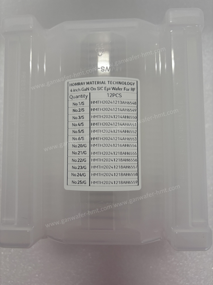
4 inch GaN on SiC Epi Wafer For RF
Project Description
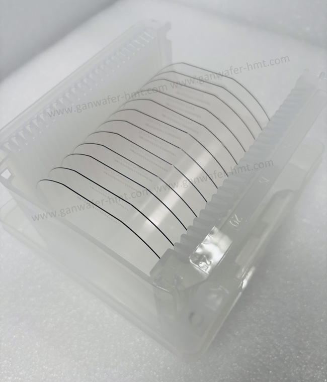
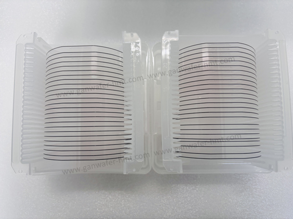
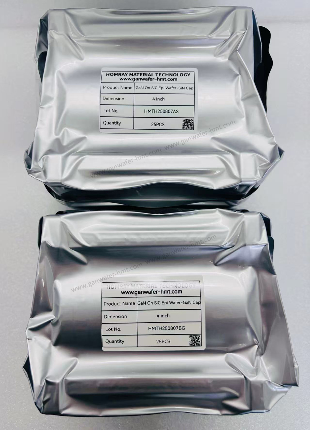
HMT can make GaN On SiC Epi Wafer for RF application. We can offer 100mm 4inch and 150mm 6inch GaN on SiC Epi Wafer. The cap layer of RF structure is SiN Cap, GaN Cap or SiN+GaN Cap. We support customize your epi wafer structure and parameters. Email us now and disscuss your project.
![]() E-mail: kim@homray-material.com;tina@homray-material.com
E-mail: kim@homray-material.com;tina@homray-material.com
HMT Silicon Carbide (SiC) Wafer Website: www.sicwafer-hmt.com