
Our company HMT currently produces 4H-silicon carbide (SiC) boules and SiC wafers primarily of the 4H polytype, with conductive types divided into semi-insulating (undoped) and N-type. SiC wafers processed from SiC crystal ingot are ideal substrates for power electronic devices, offering low ON-resistance, high breakdown voltage, high thermal conductivity, and high operating temperatures. SiC wafers can reduce switching losses, lower cooling requirements, enable device miniaturization and weight reduction, and enhance overall system performance.
The Production Process of SiC
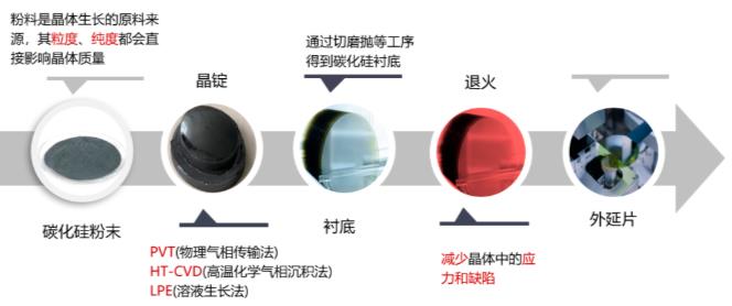
Like other power semiconductors, the silicon carbide industry chain includes crystal growth -> substrate -> epitaxy -> design -> fabrication -> packaging.
Silicon Carbide Boules
-
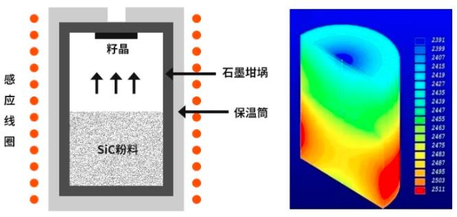
Crystal Growth
In the crystal growth stage, unlike the Czochralski process commonly used for monocrystalline silicon, silicon carbide primarily utilizes the Physical Vapor Transport (PVT) method, also known as the modified Lely method or seeded sublimation method, with the High-Temperature Chemical Vapor Deposition (HTCVD) method serving as a supplement. The core steps are roughly as follows:
Solid SiC source material -> Heating transforms the solid SiC into vapor -> Vapor transports to the seed crystal surface -> Vapor crystallizes and grows on the seed crystal surface, forming the bulk crystal.
SiC Wafer
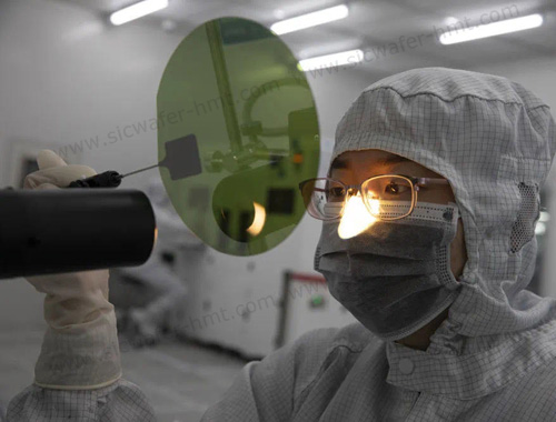
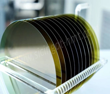
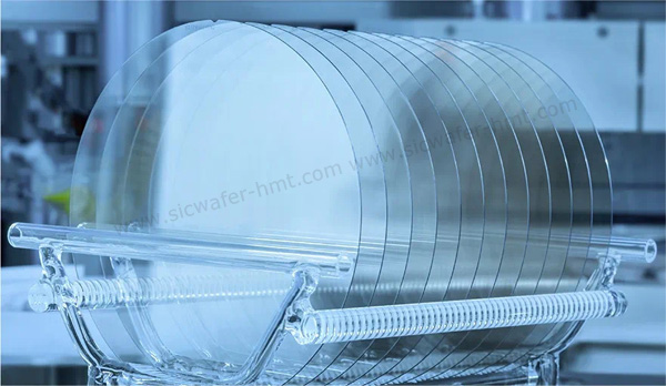
2. After crystal growth, the process moves to the wafer production stage. Through oriented cutting, grinding (rough grinding, fine grinding), polishing (mechanical polishing), and ultra-precision polishing (chemical mechanical polishing, CMP), SiC wafers are obtained. The substrate primarily provides physical support, heat conduction, and electrical conduction. The challenge in processing lies in the high hardness, brittleness, and chemical stability of SiC material, making traditional silicon-based processing methods unsuitable for SiC substrates. The quality of the cutting directly affects the performance and utilization efficiency (cost) of the SiC product, thus requiring low warp, uniform thickness, and low cutting loss. Currently, for 4-inch and 6-inch wafers, multi-wire slicing equipment is primarily used to cut the SiC crystal into thin slices with a thickness not exceeding 1mm.
Silicon Carbide Epitaxy
3. As power devices cannot be fabricated directly on the SiC substrate material, an additional epitaxial layer is required for device manufacturing. Therefore, after the substrate is completed, a specific single-crystal thin film is grown on the substrate through an epitaxial process. The substrate wafer together with the epitaxial film is called an epi-wafer. Currently, the Chemical Vapor Deposition (CVD) process is primarily used for this stage.
![]() E-mail: kim@homray-material.com;tina@homray-material.com
E-mail: kim@homray-material.com;tina@homray-material.com
HMT Silicon Carbide (SiC) Wafer Website: www.sicwafer-hmt.com