
Recently, a trend toward "12-inch SiC wafers" has emerged in China's silicon carbide (SiC) industry, with some SiC wafer manufacturers treating larger wafer sizes as a core indicator of technological breakthrough. However, based on an analysis of supply chain maturity, application requirements, and cost-effectiveness, this "size-centric" approach may lead to strategic pitfalls.
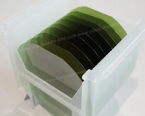
Power Device Market: The Golden Balance of 8-Inch SiC Wafers
According to Yole Développement data, the global SiC power device market was valued at approximately $2.3 billion in 2023 and is projected to reach $7.3 billion by 2028, with a compound annual growth rate (CAGR) of 27%. Even under the most optimistic growth scenarios, the SiC market remains less than 5% of the silicon semiconductor market (which was valued at around $514 billion in 2023). This scale difference means that SiC cannot replicate the "size evolution" of the silicon industry. Given that the silicon market is so large, it has taken years for 12-inch wafers to become mainstream, and 18-inch wafers are still far from widespread adoption. In contrast, the SiC market is significantly smaller, and 8-inch SiC wafers are more than sufficient to meet its needs.
More importantly, the supply chain for 8-inch SiC wafers is not yet fully mature. Currently, 8-inch materials and devices are still under development, while equipment and processes for 12-inch wafers remain largely undeveloped. Even if the SiC market grows to tens of billions of dollars in the future, 8-inch wafers are likely to remain the more economical and practical choice.
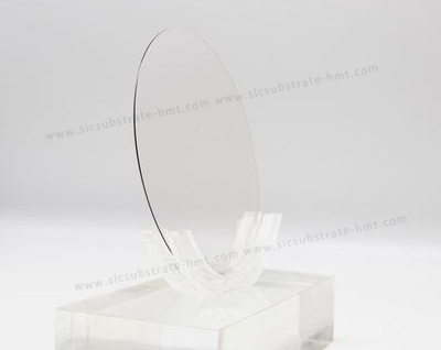
Optical Applications: 6 Inch or Smaller Wafers Are the Optimal Solution
Now, let’s consider an emerging application scenario: optical applications, such as lenses for AR glasses. This market holds significant potential. If AR glasses eventually replace smartphones as mainstream consumer electronics, the demand for SiC lenses could surpass that for power devices. Morgan Stanley predicts that the AR/VR device market could reach $1.5 trillion by 2030, with demand for SiC optical lenses potentially exceeding 30 million units per year. Contrary to intuition, larger wafer sizes present systematic disadvantages in this field.
- Low Material Utilization: AR glass lenses typically range from 2 to 3 inches in size, while wafers are circular. Cutting these small lenses from a 12-inch wafer would result in lower utilization rates, as significant material waste occurs in the center and edges of the wafer.
- Minimal Reduction in Process Costs: Optical applications involve relatively simple process steps, and costs are primarily area-dependent, particularly cutting costs. Larger wafer sizes do not significantly reduce these costs.
- Poor Optical Uniformity: Optical applications demand high uniformity in properties such as transmittance, refractive index, and stress. Larger wafers make it more difficult to ensure these properties, and defects like micropipes and inclusions, which are more prevalent in larger wafers, can adversely affect optical performance.
Thus, for optical applications, mature 6-inch SiC wafers (or even smaller sizes) are the optimal choice.
The healthy development of the SiC industry requires moving beyond "size anxiety" and establishing a technology selection framework based on scenario-specific value. Just as the essence of Moore’s Law is not the shrinking of transistor size but the exponential reduction in cost per unit, the breakthrough in the SiC industry lies not in blindly pursuing size limits but in building a technology-economic system deeply aligned with application scenarios. By deepening the mature ecosystem of 8-inch wafers in the power device field and embracing small-size wafers and new process innovations in optical applications, the industry can secure a high-value position in the global semiconductor landscape. This requires not only technical rationality but also strategic resolve. After all, the future of the industry is determined not by wafer diameter but by the precise alignment of technology and market needs.---News From ACT Compound semiconductor.
![]() E-mail: kim@homray-material.com;tina@homray-material.com
E-mail: kim@homray-material.com;tina@homray-material.com
HMT Silicon Carbide (SiC) Wafer Website: www.sicwafer-hmt.com