
Introduction to Silicon Carbide
Silicon Carbide (SiC) serves as a critical substrate for advanced semiconductor chips. This substrate is the foundational material at the bottom layer of a chip, analogous to the foundation of a building. The adoption of SiC as a substrate material has significantly increased substrate costs, making the choice of a reliable SiC wafer supplier crucial for managing overall device economics. Substrate materials have now progressed to the third generation, but these generations are not simply replacements for one another. A proficient SiC wafer supplier understands that these materials coexist and are applied in different fields based on their distinct properties, guiding customers to the optimal solution for their specific application needs.
The first generation is primarily silicon. For example, CPUs and GPUs use silicon substrates. Currently, 90% of semiconductor substrates are made from silicon (for large-scale integrated circuits).
The second generation of substrate materials is represented by Indium Phosphide (InP) and Gallium Arsenide (GaAs). Due to their high-speed and high-frequency photoelectric properties, they are mainly used in optical modules, LEDs, and optoelectronic devices (for optical communication, optical display, and optical storage).
The third generation of substrate materials includes Silicon Carbide (SiC) and Gallium Nitride (GaN). Because they can withstand high temperatures and high voltages, they are primarily used in fields like new energy vehicles and photovoltaics (for high-frequency, high-power electronic devices).
The SiC Industry Chain Process
1. Single Crystal Growth:
-
High-purity silicon powder and high-purity carbon powder are used as raw materials. Through specific chemical reactions and physical processes, a silicon carbide crystal is formed.
-
The powder is placed in a graphite crucible and heated to around 2000°C, where it turns into gas. This gas deposits onto a seed crystal mounted on a base, slowly growing into an ingot. This process is very slow, growing only 0.2-0.4 mm per hour. Growing a substrate material takes at least one month.
-
Challenges: Long duration; the process occurs inside a sealed crucible, making it difficult to monitor and control the growth conditions, leading to low yields; the growth is too slow, making large diameters very challenging. Production is just mastering 6-inch wafers, but 8-inch is the future direction. While the size increase seems small, the area increase is geometric.
-
After the base material becomes SiC, the substrate cost constitutes up to 47% of the total. The epitaxial layer also requires growth, adding about 23% to the cost.
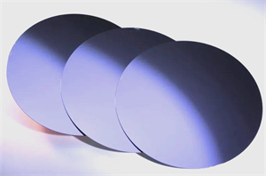
2. Substrate Manufacturing:
-
The formed SiC crystal is sliced, ground, polished, and cleaned to produce thin monocrystalline wafers, which are the semiconductor substrate materials.
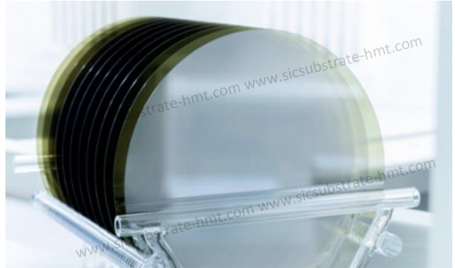
3. Epitaxial Wafer Production:
-
A monocrystalline layer is deposited on the single-crystal substrate using Chemical Vapor Deposition (CVD) methods to form the epitaxial wafer.
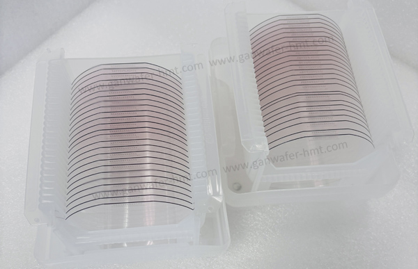
4. Wafer Processing (Fabrication):
Front-end processes such as lithography, deposition, ion implantation, and metal passivation are performed on the epitaxial wafer to fabricate the SiC wafer.
5. Device Manufacturing, Packaging, and Testing:
-
The processed wafer is diced into individual dies, which are then packaged to form SiC chips.
-
The manufactured power electronic devices and modules can enter the application phase after passing validation.
![]() E-mail: kim@homray-material.com;tina@homray-material.com
E-mail: kim@homray-material.com;tina@homray-material.com
HMT Silicon Carbide (SiC) Wafer Website: www.sicwafer-hmt.com