
What Is an Epi Ready SiC Substrate? Complete Guide for SiC Epitaxy
Introduction
With the rapid development of electric vehicles, renewable energy systems, high-frequency communication and advanced power electronics, silicon carbide (SiC) has become one of the most important wide bandgap semiconductor materials. Among different types of SiC wafers, Epi Ready SiC Substrates play a critical role because they provide a highly optimized surface for epitaxial layer growth.
Unlike standard SiC substrates, epi ready SiC substrates undergo advanced surface preparation processes to achieve ultra-low surface roughness, excellent flatness and improved surface cleanliness, creating an ideal foundation for manufacturing high-performance SiC semiconductor devices. For advanced applications, Homray provides 4 inch Epi Ready SiC Substrates designed for reliable SiC epitaxy, MOSFET fabrication and RF device production.
1. What Is an Epi Ready SiC Substrate?
An Epi Ready SiC Substrate is a silicon carbide wafer that has been specially processed and polished to meet the strict requirements of epitaxial growth.
During semiconductor manufacturing, an epitaxial layer is deposited on the SiC substrate surface through processes such as chemical vapor deposition (CVD). The quality of the substrate surface directly affects the uniformity, defect density and performance of the final semiconductor device.
Compared with conventional SiC wafers, epi ready substrates typically provide:
a. Ultra-smooth polished surface
b. Low surface defect density
c. Excellent thickness uniformity
d. Reduced surface damage
e. High crystal quality
f. Clean contamination-free surface
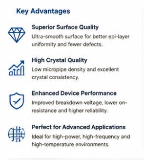

These characteristics make epi ready SiC substrates suitable for next-generation semiconductor manufacturing.
2. Structure of a SiC Epitaxy System
The typical structure of a SiC power device includes several layers:
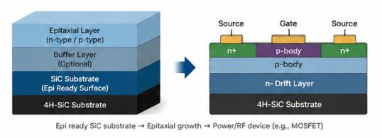
3. How Does SiC Epitaxy Work?
The SiC epitaxy process generally includes several steps:
Step 1: Surface Preparation
The epi ready SiC wafer surface is cleaned to remove particles, contamination and surface damage.
Step 2: Epitaxial Growth
A high-quality SiC epitaxial layer is grown on the substrate using CVD technology.
The epitaxial layer thickness and doping concentration can be precisely controlled according to device requirements.
Step 3: Quality Inspection
The wafer is inspected for: Surface morphology / Thickness uniformity / Defect density/ Crystal quality
Step 4: Device Fabrication
The epi wafer is processed into semiconductor devices including: SiC MOSFETs / Schottky diodes / Power modules / RF devices

4. Why Choose 4H-SiC Epi Ready Substrate?
Superior Electrical Performance
4H-SiC provides:
- Wide bandgap
- High breakdown field
- High thermal conductivity
These advantages allow semiconductor devices to operate under higher voltage, higher temperature and higher frequency conditions.
Improved Epitaxial Layer Quality
A high-quality epi ready surface helps reduce:
- Micropipe defects
- Surface irregularities
- Epitaxy defects
This improves manufacturing yield and device reliability.
Better Thermal Management
SiC has excellent thermal conductivity compared with traditional silicon materials, making it ideal for high-power applications.
 E-mail: kim@homray-material.com;tina@homray-material.com
HMT Silicon Carbide (SiC) Wafer Website: www.sicwafer-hmt.com