
A GaN HEMT (Gallium Nitride High Electron Mobility Transistor) is a high-performance power semiconductor device whose performance begins with the core material—the GaN epi wafer. GaN Epi Wafer Manufacturer HMT produces these critical wafers by growing a thin layer of Aluminum Gallium Nitride (AlGaN) on a high-quality Gallium Nitride (GaN) layer. This structure spontaneously generates a Two-Dimensional Electron Gas (2DEG) at the interface, which enables extremely high electron mobility. This allows GaN HEMTs to switch faster and operate more efficiently than traditional silicon transistors. Enhanced-mode (eMode) GaN HEMTs, commonly found in modern fast-chargers, are the preferred type for their safety, driven by advanced epi wafers from manufacturers like HMT.
Currently, there are two main types of mature GaN devices on the market:
Enhanced-Mode (E-Mode): Normally in the "off" state, it requires a voltage to turn "on." Safer and more commonly used.
Depletion-Mode (D-Mode): Normally in the "on" state, it requires a voltage to turn "off." More complex to use, as it requires additional circuitry.
Most everyday products, such as chargers, use enhanced-mode devices.
Ingenious Fabrication: From Substrate to Heterojunction
 GaN devices are typically manufactured using the "heteroepitaxial method." This may sound complex, but it can be broken down step by step:
Laying the Foundation (Substrate): First, a silicon (Si) wafer is used as the substrate.
Buffer Layer: Growing gallium nitride directly on silicon would cause lattice mismatch due to differences in atomic spacing. Therefore, a buffer layer is grown first using methods like vapor-phase epitaxy to perfectly bridge this discrepancy.
Growing the Core Material: On the smooth buffer layer, high-quality gallium nitride (GaN) crystal layers can be grown.
A single GaN layer is unremarkable and may not even conduct electricity. However, the genius lies in growing an ultra-thin layer of aluminum nitride (AlN) or aluminum gallium nitride (AlGaN) on top. When these two materials combine, a remarkable phenomenon occurs!
Two-Dimensional Electron Gas (2DEG)
At the interface where the two materials meet, a highly concentrated and fast-moving two-dimensional electron gas (2DEG) spontaneously forms without any artificial doping. This is the key to the high performance of GaN HEMTs! How does it occur?
This is primarily attributed to two physical effects:
Piezoelectric Polarization Effect: To match the lattice of GaN, the AlN layer undergoes "stretching" and "compression," generating an internal electric field (piezoelectric field). This field acts like an invisible hand, pushing electrons toward the interface.
Spontaneous Polarization Effect: Materials like GaN and AlN inherently have an internal electric field due to the misalignment of their positive and negative charge centers.
However, these factors alone are not sufficient. The most critical aspect is the presence of "trap states" on the surface of AlN (which can be thought of as holes or pits). To fill these "pits" and minimize the system's energy, free electrons continuously gather at the interface.
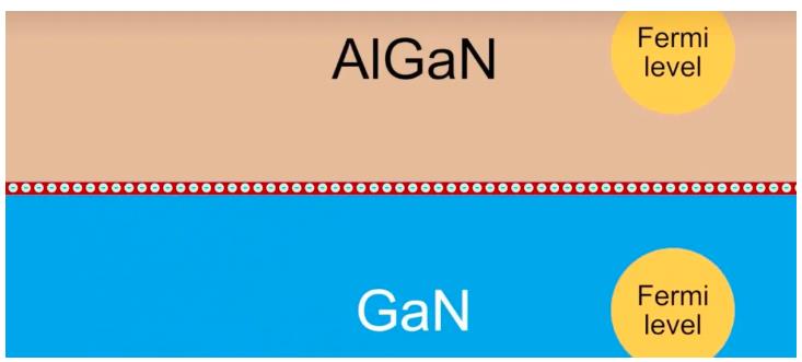
Ultimately, under the combined influence of the piezoelectric field and energy band bending, a large number of free electrons are "confined" at the interface between GaN and AlN. These electrons can move freely within this two-dimensional plane (left, right, forward, backward) but cannot escape upward or downward, hence the name "two-dimensional electron gas."
How Is Switching Controlled?
Once the 2DEG is formed, the device is normally conductive (depletion-mode). However, what we need is an enhanced-mode device that is normally off and turns on when voltage is applied, as this is safer.
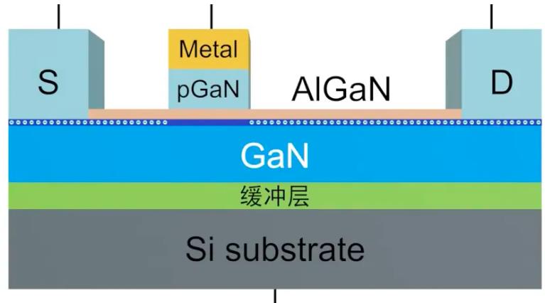
 To achieve this, a P-type GaN layer is added below the gate.This material is doped with specific atoms, creating numerous "holes" (positive charges) inside.It forms a PN junction directly below, and the electric field of this junction "repels" the nearby 2DEG, creating an "interruption region" beneath the gate.
This completes the design of an enhanced-mode device:
When the gate voltage is 0: The interruption region exists, the 2DEG channel is disconnected, and the circuit cannot conduct.
When a positive voltage is applied to the gate: This voltage counteracts the repelling effect of the PN junction, eliminating the interruption region and reconnecting the 2DEG channel, allowing the circuit to conduct.
By simply controlling the gate voltage like a water tap switch, we can efficiently manage the operation of the entire circuit.
![]() E-mail: kim@homray-material.com;tina@homray-material.com
E-mail: kim@homray-material.com;tina@homray-material.com
HMT Silicon Carbide (SiC) Wafer Website: www.sicwafer-hmt.com