
Silicon Carbide (SiC) Wafer Cutting Technology is the critical process of slicing a SiC ingot along specific crystallographic directions into thin wafers. The primary goal for any SiC wafer manufacturer is to produce wafers with minimal warpage and uniform thickness, which are essential for high-performance semiconductor devices. As a leading SiC wafer manufacturer, HMT utilize advanced processes to ensure the highest quality standards from ingot to wafer.
Currently, the primary methods for cutting monocrystalline SiC wafers include diamond bade cutting, wire electrical discharge machining (WEDM), wire saw cutting, laser thermal stress-controlled fracture cutting (laser cleaving), and laser stealth dicing.
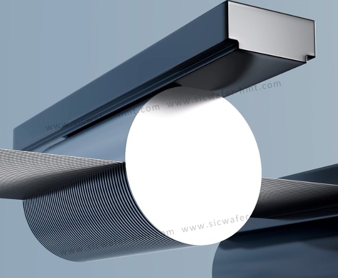
Wire Saw Cutting
Diamond Wire Saw Cutting
Diamond wire saw cutting technology involves bonding high-hardness, high-wear-resistant diamond abrasive grains to the cutting wire via methods like electroplating, resin bonding, brazing, or mechanical embedding. Cutting is accomplished through the high-speed motion of the diamond wire.
Based on the motion of the diamond wire, it can be categorized into three types: unidirectional, reciprocating, and looped. Comparatively, reciprocating and looped fixed diamond wire saws have a longer effective length and higher reuse rate per unit length of the wire, leading to higher cutting efficiency. They are now widely used in the field of hard and brittle material cutting and have become the mainstream process for SiC wafer cutting.
Unlike the "three-body" (involving wire, abrasive, workpiece) of loose abrasive wire saw cutting, diamond wire saw cutting belongs to "two-body" (wire with abrasives vs. workpiece). Its processing efficiency is several times higher than that of loose abrasive wire saw cutting. However, it still has significant drawbacks: large kerf width, relatively high surface roughness, and material loss as high as 46%. The kerf is typically above 200μm, making it less suitable for producing ultra-thin, large-diameter SiC monocrystalline wafers.
Laser Cutting Methods
Laser cutting technology has been applied early on for silicon ingot cutting and is just starting to be used in the SiC field. Current main laser techniques include water-jet guided laser, KABRA, cold cutting, and modified layer cutting.
Water-Jet Guided Laser Cutting (Surface Cutting)
Water-jet guided laser (LMJ) cutting technology, also known as laser microjet technology, works by focusing a laser beam into a nozzle, passing it through a pressure-modulated water chamber, and then ejecting a low-pressure water jet. Due to the difference in refractive index between water and air, an optical waveguide is formed at the water-air interface, allowing the laser to propagate along the direction of the water flow, thus guided by the high-pressure water jet to cut the material surface.
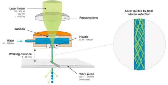
- The advantages of this technology are:The water flow cools the cutting zone, reducing thermal deformation and thermal damage to the material.
-
Significantly faster cutting speed.
-
The ejected water stream carries away machining debris and contaminants.
-
The water-jet fiber has a large working distance and requires no laser focusing on the workpiece.
-
The small water jet diameter reduces kerf width, improves machining precision, and results in smoother cut surfaces.
KABRA Dicing (Stealth Dicing)
The KABRA (key amorphous-black repetitive absorption) technology from Japan's DISCO Corporation is a more advanced laser cutting technique. KABRA technology uses an optical system with excellent focusing capability to transmit the laser through the surface of the SiC and focus it inside the wafer, forming a modified layer at specific depths. After forming this layer, wafers can be separated from the ingot.
KABRA technology is more suitable for large-diameter wafer cutting but is protected by strict patents. The KABRA process is relatively mature, offering advantages like reduced material loss and increased cutting speed, thereby improving slicing efficiency, and is more suitable for large-diameter wafer applications. However, KABRA is technologically challenging, with risks of exacerbating wafer breakage during process refinement, and is protected by stringent patents, making it difficult for domestic manufacturers to replicate.
Cold Cutting
The cold cutting process primarily involves two technical steps: First, laser irradiation creates an exfoliation layer inside the SiC ingot, causing volumetric expansion of the material and generating tensile stress to form a very narrow layer of micro-cracks. Then, a polymer cooling step processes these micro-cracks into a main crack, ultimately separating the wafer from the remaining ingot.
- The advantages of this technology are:Total kerf loss per wafer is less than 100μm.
- Yield of SiC wafers can be increased by up to 90%.
- This technology significantly reduces raw material loss during SiC wafer production, potentially yielding up to 3 times more usable material from an ingot. Ultimately, SiC device production capacity can increase by nearly 2 times, with costs reduced by 20-30%.
Modified Layer Cutting (QCB/Stealth Dicing-like)
Modified layer cutting is a laser technology for rapidly separating a SiC ingot into individual wafers, also known as QCB (Quasi-Cleaving/Breaking). The process involves using a picosecond laser beam to form a modified layer inside the ingot, enabling wafers to be precisely separated along the laser-scanned path with minimal external force. Currently, Han's Laser's SiC ingot laser slicing machine is undergoing customer validation in China.
SiC modified layer cutting generally involves two main steps: laser scanning and mechanical cleaving based primarily on the three-point bending principle. Laser scanning forms the modified layer, where the laser precisely induces micro-cracks at specified positions inside the material. When these uniformly distributed micro-cracks exist, they cause stress fields (thermal stress, mechanical stress, etc.) to concentrate around them. When the mechanical cleaving applies bending stress, the presence of the modified layer guides the stress to the specified location, promoting crack propagation and enabling precise separation of the wafer.
![]() E-mail: kim@homray-material.com;tina@homray-material.com
E-mail: kim@homray-material.com;tina@homray-material.com
HMT Silicon Carbide (SiC) Wafer Website: www.sicwafer-hmt.com