
SiC Wafer Quality Control and Quality Management System
For silicon carbide substrates, consistent material quality is essential to the performance and repeatability of downstream semiconductor processes. HMT manages SiC wafer quality through a structured quality control system covering material evaluation, wafer processing, surface inspection, dimensional verification, final inspection and product traceability.
Rather than relying on final inspection alone, our quality approach focuses on process consistency, defect prevention and specification control throughout wafer manufacturing. Customer requirements are reviewed before production, while key characteristics are monitored at appropriate stages of processing.
Quality Control Across the SiC Wafer Manufacturing Process
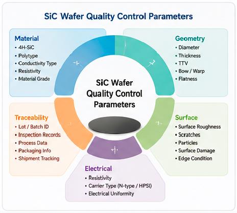 HMT's quality management approach is organized around several critical control stages:
1. Material and Incoming Quality Control
The quality of the starting material has a direct influence on the characteristics of the finished SiC substrate. Incoming materials are evaluated according to the applicable project requirements before entering subsequent processing steps.
Depending on the wafer specification, quality considerations may include crystal material, polytype, conductivity type, material grade and other customer-defined parameters.
The quality of the starting material influences subsequent wafer processing, and customers requiring upstream SiC material can also review our SiC boule and ingot options.
2. Wafer Processing Control
SiC wafers pass through multiple processing stages before reaching the required final specification. Process parameters are controlled to maintain consistency between production batches and reduce variations that may affect the finished substrate.
Key process areas can include wafer slicing, grinding, lapping, polishing, cleaning and surface preparation.
For projects requiring specific wafer dimensions or substrate conditions, customer specifications are incorporated into the production and inspection process.
3. Surface and Appearance Inspection
Surface condition is an important quality factor for polished SiC substrates. Inspection procedures are used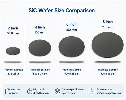 to identify visible surface abnormalities and other characteristics that may affect subsequent semiconductor processing.
The inspection criteria are defined according to the applicable product specification and customer requirements.
SiC Wafer Dimensional and Geometrical Control
Wafer geometry is another important part of substrate quality. Diameter, thickness and other dimensional characteristics need to remain within the agreed specification to support consistent downstream processing.
HMT can control and inspect parameters such as:
# Wafer diameter
# Wafer thickness
# Thickness tolerance
# Wafer orientation
# Bow and warp
# Other customer-defined dimensional requirements
SiC Wafer Defect Inspection
Defect control is an important part of silicon carbide substrate manufacturing because crystal and surface-related defects can influence subsequent device fabrication.
HMT's quality process therefore considers both material-related characteristics and wafer-surface conditions. Inspection requirements can be adapted to the intended application and product grade.
Quality Control for 2 Inch to 8 Inch SiC Wafers
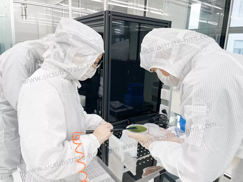
HMT supports multiple SiC wafer diameters, including 2 inch, 4 inch, 6 inch and 8 inch substrates. Each wafer size can have its own dimensional and process-control requirements.
For customers selecting a substrate size for research or semiconductor development, the appropriate quality specification can be established according to wafer diameter, material type, surface condition and intended process.
For smaller-scale semiconductor research and prototype development, HMT provides 2 inch 4H-SiC wafers with conductive N-type material and project-specific specifications. For larger substrate requirements, HMT also supplies 4 inch 4H-SiC wafers for semiconductor development and production-oriented processes.
Continuous Improvement in SiC Wafer Quality
Quality management is an ongoing process rather than a single final inspection step. Production feedback, inspection results and customer requirements can be reviewed to identify opportunities for process improvement.
HMT uses a continuous-improvement approach to strengthen process stability, inspection consistency and customer-specific quality control.
 E-mail: kim@homray-material.com;tina@homray-material.com
HMT Silicon Carbide (SiC) Wafer Website: www.sicwafer-hmt.com