
Trusted SiC Substrate Manufacturers HMT focus on producing silicon carbide wafers, a compound semiconductor formed by covalent bonds between silicon and carbon. It exhibits properties such as a wide bandgap (enabling high-temperature resistance), high thermal conductivity (suitable for high power handling), a high breakdown electric field (providing high-voltage resistance), and a high electron saturation drift velocity (ideal for high-frequency operation).
Classification by size: 4 inch 6 inch (mainstream in the market), 8 inch (gradually entering mass production). Classification by substrate type:
(1) Conductive SiC substrates: Good conductivity, used for power devices, such as vehicle power supplies, DC charging stations, photovoltaic/storage inverters, and industrial power supplies.
(2) Semi-insulating SiC substrates: Nearly non-conductive, used for radio frequency devices, such as communication base stations (power amplifiers) and radar systems.
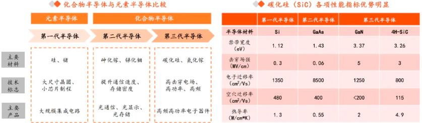
Semiconductor materials are categorized into generations: first-generation silicon and germanium; second-generation gallium arsenide (GaAs) and indium phosphide (InP); and third-generation silicon carbide (SiC) and gallium nitride (GaN).
CoWoS Technology
TSMC’s CoWoS process is a 2.5D advanced packaging technology. Its core lies in integrating the GPU and HBM within the same package using an interposer, enabling ultra-high bandwidth and low-latency inter-chip communication.
In the CoWoS structure (chip layer–interposer–substrate layer), the interposer connects the chip layer (GPU, HBM) with the substrate, achieving high-density signal interconnections.
Traditional interposers use silicon as the base material. Silicon carbide, as a third-generation wide-bandgap semiconductor material, exhibits significantly superior properties such as thermal conductivity compared to silicon, making it particularly suitable for high-power, highly integrated AI chips.
NVIDIA’s high-end GPUs all employ CoWoS. To further enhance performance, NVIDIA plans to replace the interposer material in CoWoS with a silicon carbide substrate, and TSMC is actively advancing related R&D efforts.
Preparation Process and Workflow
SiC particles undergo a series of processes to prepare substrates, followed by epitaxial growth to form an epitaxial layer, meeting the electrical performance requirements of downstream devices.
 3.1 Substrate Preparation
(1) Raw material synthesis: High-purity silicon powder and carbon powder react to synthesize silicon carbide particles. The mainstream method is the carbothermal reduction process.
(2) Crystal growth: Silicon carbide powder undergoes sublimation and deposition at high temperatures, growing into an ingot on a seed crystal. The mainstream method is the physical vapor transport (PVT) process.
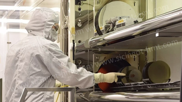
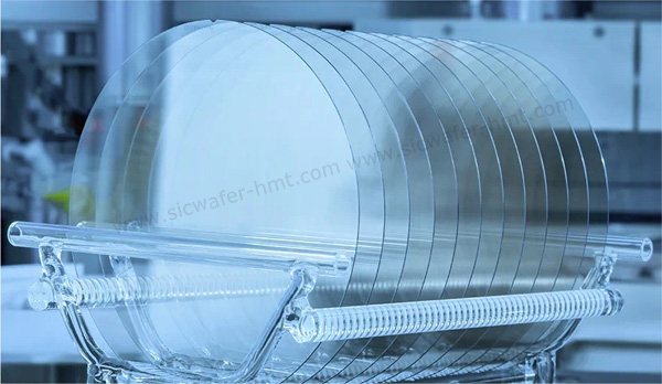
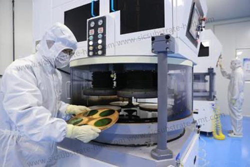
(3) Substrate processing: The ingot undergoes slicing, grinding, polishing, cleaning, and other steps to produce thin silicon carbide substrate wafers of standard diameters.
3.2 Epitaxial Growth
(1) Substrate pretreatment: Lattice defects are repaired through in-situ etching and high-temperature annealing.
(2) Epitaxial growth: The chemical vapor deposition (CVD) method is used to deposit a single-crystal thin film (epitaxial layer) on the surface of the silicon carbide substrate. Its doping type determines the functionality of the device.
![]() E-mail: kim@homray-material.com;tina@homray-material.com
E-mail: kim@homray-material.com;tina@homray-material.com
HMT Silicon Carbide (SiC) Wafer Website: www.sicwafer-hmt.com