
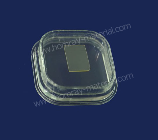
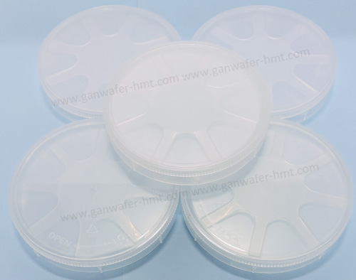
Square Free-Standing GaN Substrate
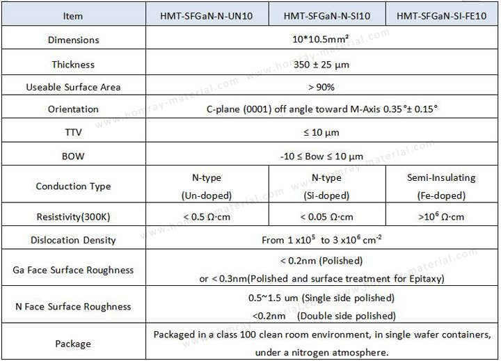
Dimension:10*15mm²
Thickness: 350±25um
Useable Surface Area:>90%
Conduction Type: N Type,SI Type
Product Description
As the leading manufacturer and supplier of Free-Standing GaN Substrate wafer, Homray Material Technology can provide 10*15mm² square Free-Standing GaN Substrate wafer with Un-doped N type,Si doped N type and Fe doped Semi-Insulating type. Due to GaN(Gallium Nitride) unique characteristics:high maximum current, high breakdown voltage, and high switching frequency), Gallium Nitride (GaN) is the unique material of choice to solve energy problems of the future. GaN based systems have higher power efficiency, thus reducing power losses, switch at higher frequency, thus reducing size and weight.
GaN technology is used in numerous high-power applications such as industrial, consumer and server power supplies, solar, AC drive and UPS inverters, and hybrid and electric cars. Furthermore, GaN is ideally suited for RF applications such as cellular base stations, radars and cable TV infrastructure in the networking, aerospace and defense sectors.
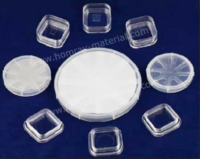
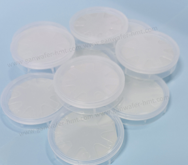
Related Products
![]() E-mail: kim@homray-material.com;tina@homray-material.com
E-mail: kim@homray-material.com;tina@homray-material.com
HMT Silicon Carbide (SiC) Wafer Website: www.sicwafer-hmt.com