
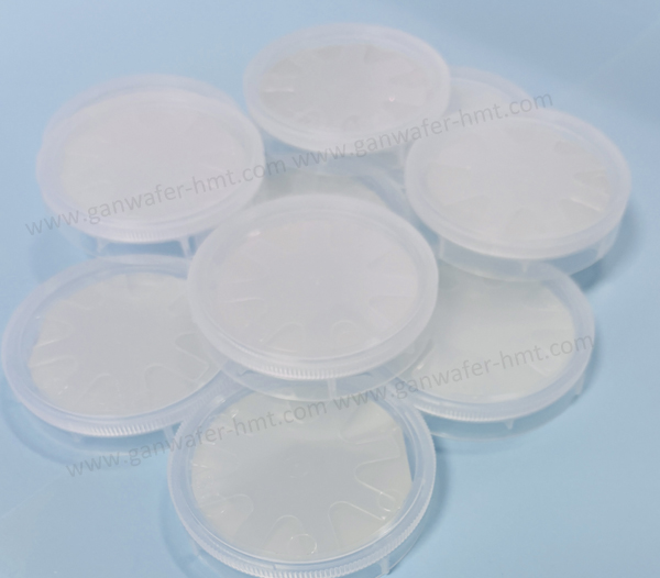
2 Inch Free-Standing GaN Substrate
Dimensions: Ф 50.8 mm ± 1 mm
Thickness: 350 ± 25 µm
Useable Surface Area: > 90%
Total Thickness Variation: ≤ 15 µm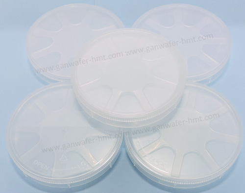
4 Inch Free-Standing GaN Substrate
Dimensions: Ф 100 mm ± 1 mm
Thickness: 400 ± 50 µm
Useable Surface Area: > 90%
Total Thickness Variation: ≤ 40 µm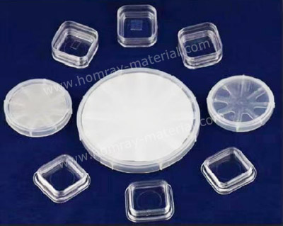
Square Free-Standing GaN Substrate
Dimension:10*15mm²
Thickness: 350±25um
Useable Surface Area:>90%
Conduction Type: N Type,SI Type
Home<<1
>>Last
![]() E-mail: kim@homray-material.com;tina@homray-material.com
E-mail: kim@homray-material.com;tina@homray-material.com
HMT Silicon Carbide (SiC) Wafer Website: www.sicwafer-hmt.com