
4 inch 4H-SiC Wafer Manufacturer
Diameter: 100±0.2mm
Grade: Production
Thickness: 350±25um
Type: Conductive N
Product Description
Trusted global SiC Wafer Manufacturer HMT company offer P grade 4 inch SiC Wafers both Conductive N type (off axis) and Semi-insulating SI type (on axis). We have SiC Wafer production line: crystal growth, crystal processing, wafer processing, polishing, cleaning and testing. Our 4 inch SiC Wafers have low micropipe densitiy and good technical parameters. We will provide best price for you. Contact us and disscuss your project now!
4 inch SiC Wafer Spec
| Item | Spec |
| Diameter | 100±0.25mm |
| Orientation | 4° toward <11-20> ± 0.5º |
| Thickness | 350±25um |
| Dopant | Nitrogen |
| Primary flat orientation | [1-100]± 5° |
| Micropipe density | ≤ 0.5 ea/cm² |
| TTV | ≤ 10um |
| BOW | -25~25um |
| Surface finish | Si-face CMP/ C-face polished |
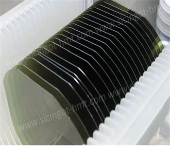
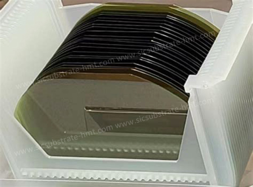
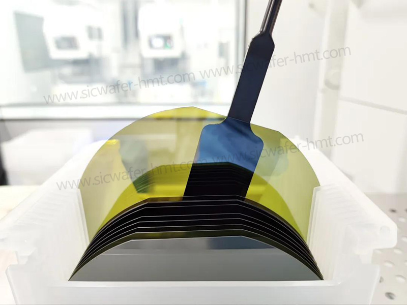
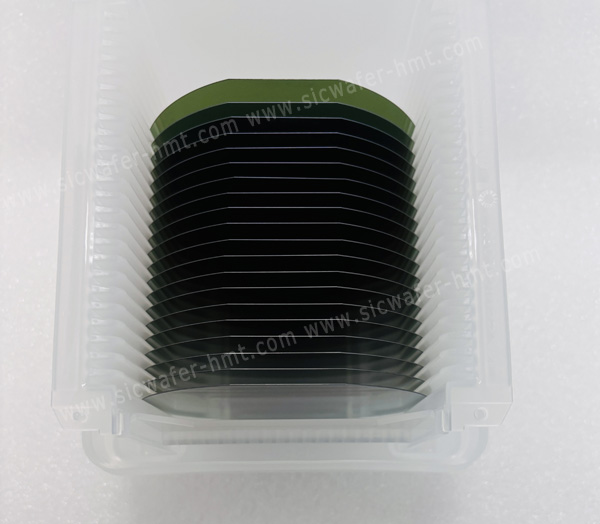
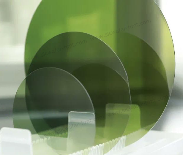
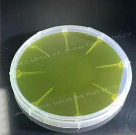
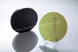
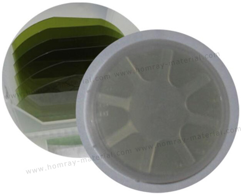
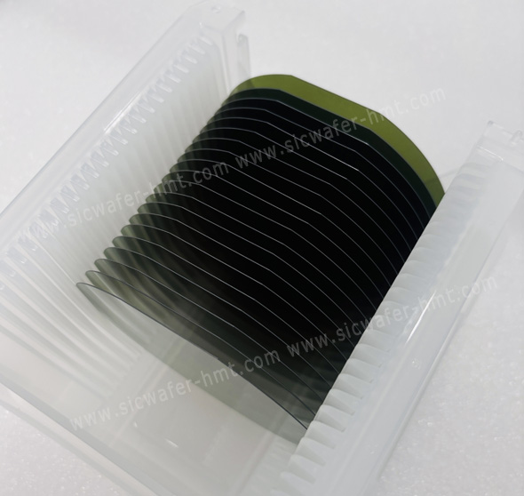
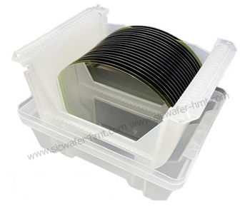
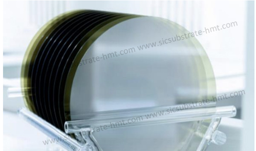
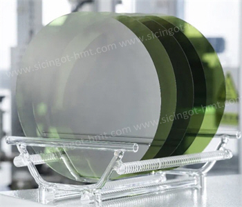
SiC Wafer Pictures
Core Characteristics and Value of SiC
Silicon carbide (SiC) materials exhibit significantly superior performance compared to traditional silicon-based semiconductors in high-frequency, high-voltage, and high-temperature applications. Its core value lies in:
Improving Energy Efficiency: Reducing energy loss during conversion, such as extending the range of electric vehicles or increasing the conversion efficiency of photovoltaic inverters.
Reducing Size: High-frequency characteristics allow for the use of smaller passive components, making systems lighter and more compact.
Enhancing Reliability: High-temperature stability and excellent thermal conductivity contribute to stable operation in harsh environments and simplify thermal management design.
Applications of SiC Products
*New Energy Vehicles (Core Driver)
*Photovoltaics and Energy Storage
*Industrial Control and Smart Grid
*Communications and Data Centers
*Consumer Fast Charging and Rail Transportation
Related Products
![]() E-mail: kim@homray-material.com;tina@homray-material.com
E-mail: kim@homray-material.com;tina@homray-material.com
HMT Silicon Carbide (SiC) Wafer Website: www.sicwafer-hmt.com