
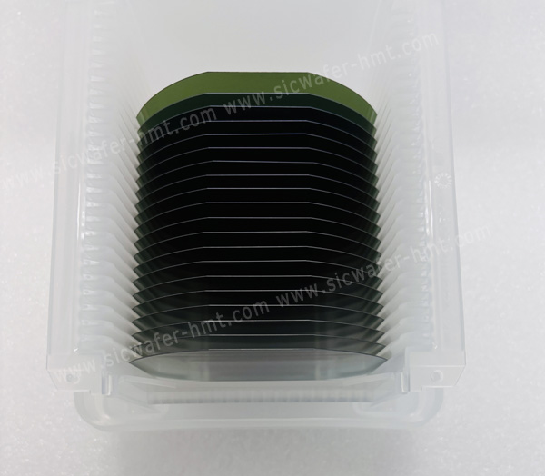
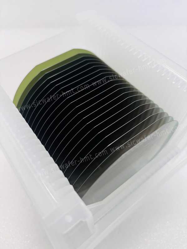
Epi ready 4 inch SiC Substrate manufacturers
Diameter: 100mm
Grade: Production
Thickness: 350um/500um
Type: Conductive N, HPSI
Product Description
Epi Ready 4 inch SiC Substrate for Advanced Semiconductor Manufacturing
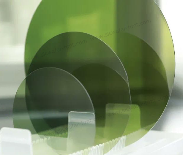
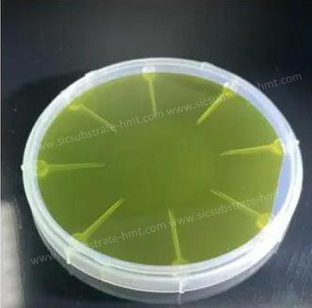
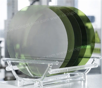
HMT is a professional manufacturer of Epi Ready 4 inch SiC Substrates, providing high-quality 100mm silicon carbide substrates designed for advanced epitaxial growth processes. Our 4H-SiC substrates feature optimized surface morphology, excellent crystalline quality and stable performance for next-generation semiconductor devices.
Unlike standard SiC wafers used for general applications, Epi Ready SiC substrates are specially processed to meet the strict requirements of epitaxial layer growth. The ultra-smooth surface and controlled wafer quality help improve epitaxy uniformity, reduce defect impact and enhance device reliability.
Our 4 inch SiC Epi Ready Substrates are widely used as a foundation material for SiC power devices, including MOSFETs, Schottky diodes, high-voltage switching components and advanced RF semiconductor structures.
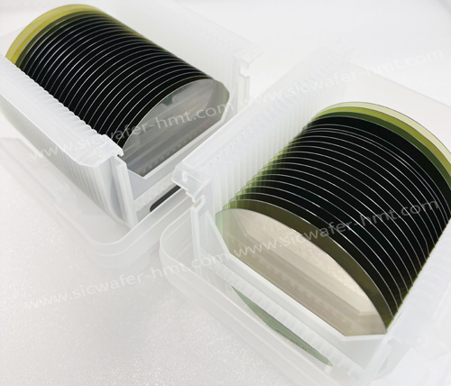
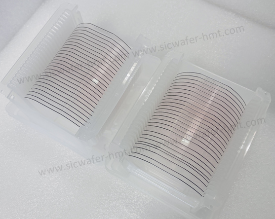
Key Features of 4 inch SiC Epi Ready Substrate
High Quality Epitaxy Surface
The substrate surface is optimized through precision polishing technology to provide a suitable platform for SiC epitaxial layer growth. Low surface roughness enables better epi-layer uniformity and improves device fabrication consistency.
4H-SiC Crystal Structure
The 4H-SiC polytype provides excellent electrical and thermal properties, making it the preferred substrate material for high-power and high-frequency semiconductor applications.
Reliable Wafer Performance
Each wafer undergoes strict quality inspection to ensure stable thickness control, surface cleanliness and crystal quality for semiconductor manufacturing processes.
Customized Specifications Available
HMT supports customized requirements including conductivity type, thickness, surface treatment and wafer specifications according to customer epitaxy process requirements.
Product Specifications
| Parameter | Specification |
| Product | Epi Ready 4 inch SiC Substrate |
| Material | Silicon Carbide (SiC) |
| Diameter | 4 inch (100mm) |
| Polytype | 4H-SiC |
| Conductivity Type | N-type / Semi-insulating |
| Surface | Epi-ready polished surface |
| Thickness | 350um/500um |
| Orientation | 4° off-axis or 0° on-axis |
| Application | SiC Epitaxy, MOSFET, SBD, RF Devices |
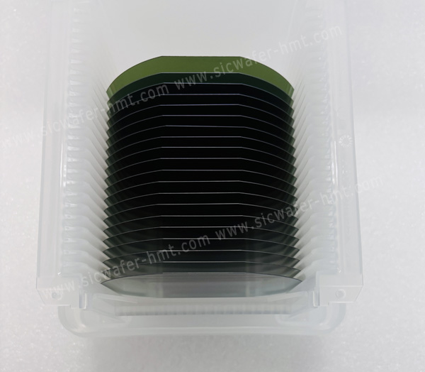
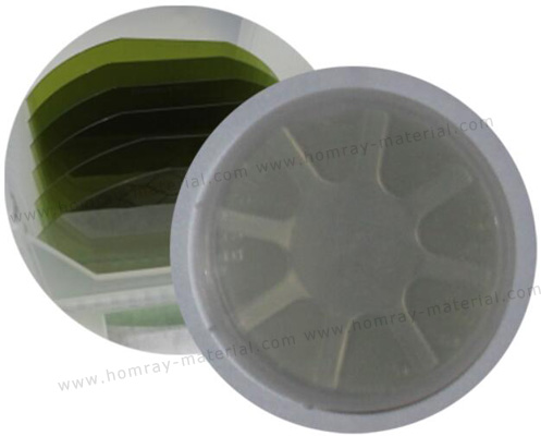
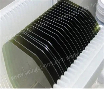
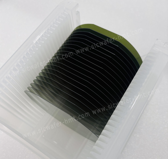
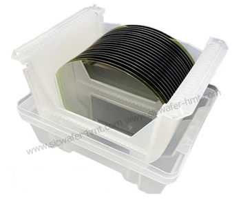
| Package | 25PCS in one cassette |

Why Choose HMT as Your SiC Substrate Supplier
HMT focuses on the development and manufacturing of wide bandgap semiconductor materials, including SiC substrates, SiC epitaxial wafers and GaN-related semiconductor products. With advanced wafer processing capability and strict quality control, HMT provides reliable substrate solutions for global semiconductor customers.
Our Epi Ready 4 inch SiC substrates help customers achieve:
- Improved epitaxial growth consistency
- Reduced wafer processing risks
- Better device performance
- Stable supply for research and mass production
What is an Epi Ready SiC Substrate?
An Epi Ready SiC Substrate is a silicon carbide wafer specially processed with a high-quality polished surface designed for epitaxial layer growth. It provides an ideal foundation for manufacturing SiC semiconductor devices.
What applications use 4 inch SiC Epi Ready Substrates?
4 inch SiC Epi Ready Substrates are mainly used for SiC MOSFETs, Schottky diodes, power modules, RF devices and other wide bandgap semiconductor applications.
Related Products


 E-mail: kim@homray-material.com;tina@homray-material.com
HMT Silicon Carbide (SiC) Wafer Website: www.sicwafer-hmt.com