
GaN Epitaxial On SiC For Power HEMT
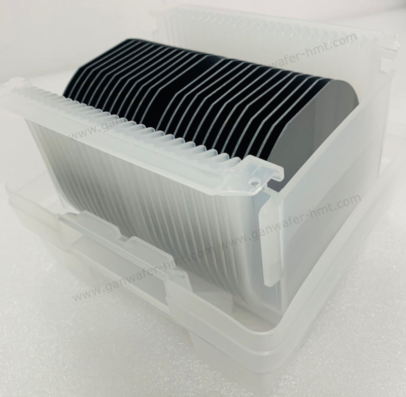
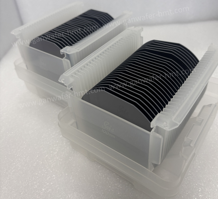
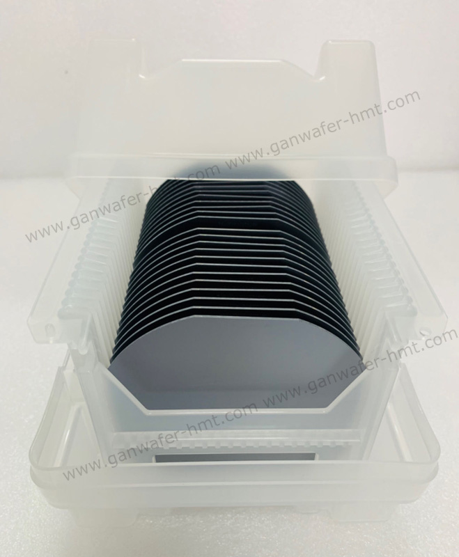
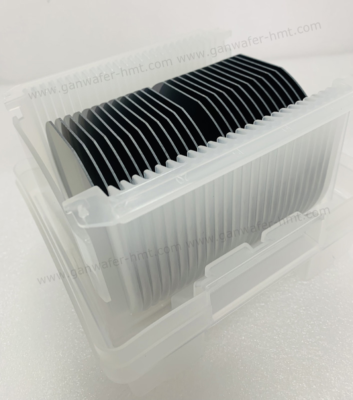
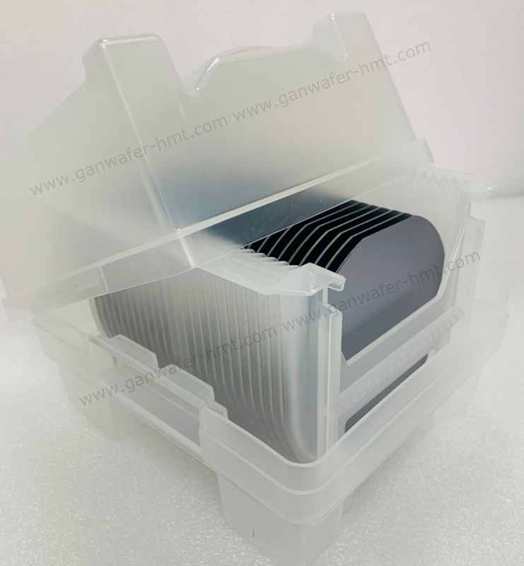
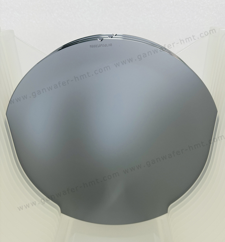
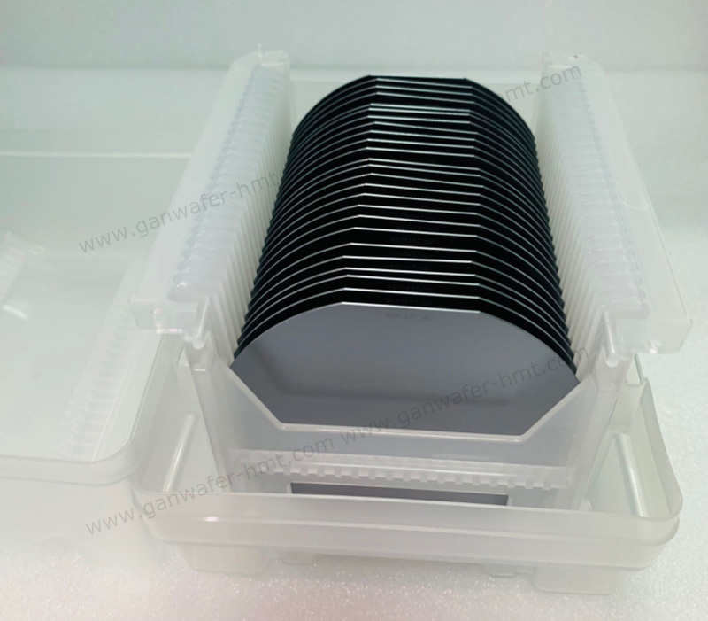
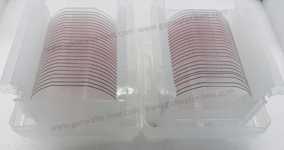
GaN-On-SiC Epi Wafer For Power HEMT
Substrate Size: 4 inch,6 inch
Substrate Thickness: 500um
GaN Buffer Layer: 2-3um
Product Description
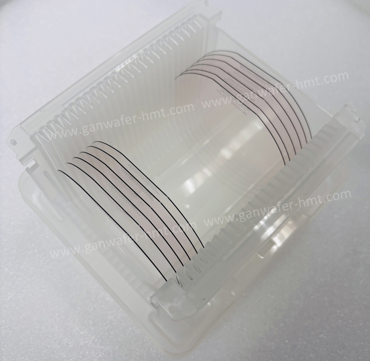
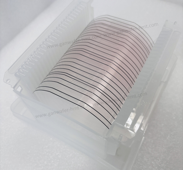
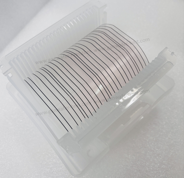
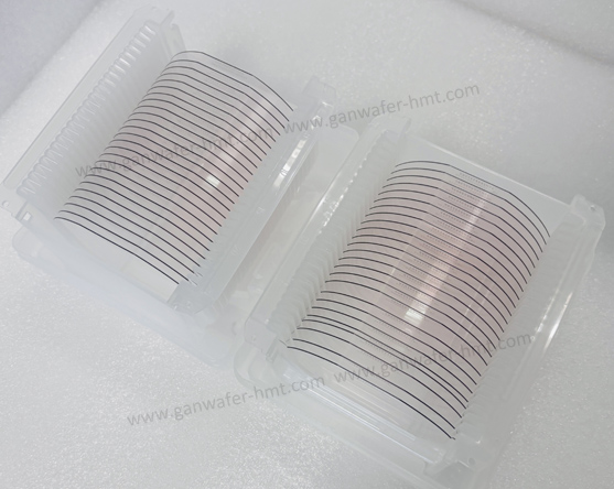
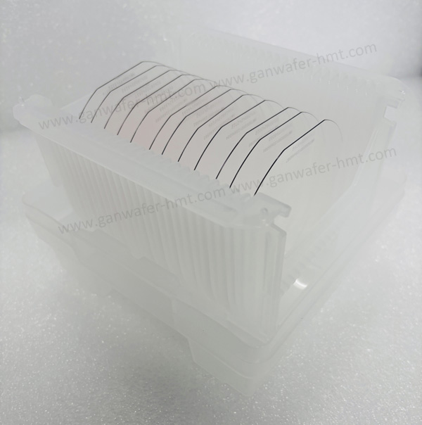
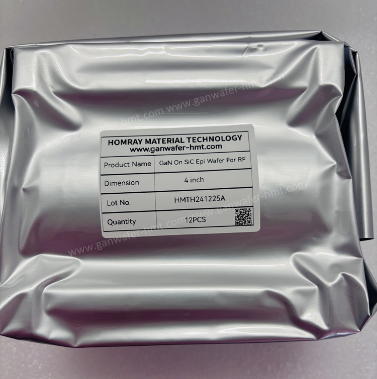
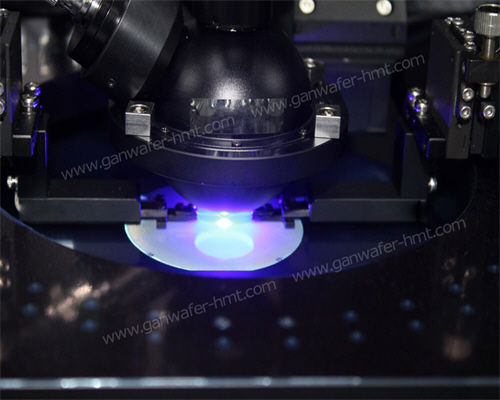
Homray Material Technology manufactures GaN-on-SiC and GaN-on-Si Epitaxial wafer and supplies these GaN Epi Wafers to integrated device manufacturers to create high performance power and RF devices.Our GaN-on-SiC Epi Wafer can be divided into Power HMET structure and RF HEMT structure. 4 inch and 6 inch both available in HMT and each layer structure can be customized.
GaN Epi Wafer Application
RF applications such as power amplifier
Vehicle power devices
Power electronics such as power supplies, DC/DC converter, etc.
Environment resistant devices
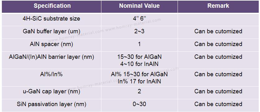
Standard Layer Specification For Power HEMT
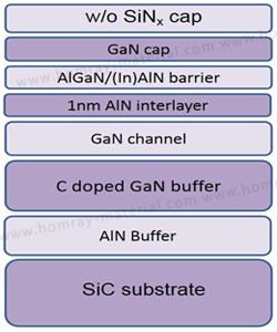
Standard Layer Structure
Related Products
![]() M.P: +86-15366208370 ; +86-15366203573
M.P: +86-15366208370 ; +86-15366203573
![]() E-mail: kim@homray-material.com;tina@homray-material.com
E-mail: kim@homray-material.com;tina@homray-material.com
HMT Silicon Carbide (SiC) Wafer Website: www.sicwafer-hmt.com