
GaN Epitaxial (Epi) Wafer Manufacturers
RF and Power HEMT
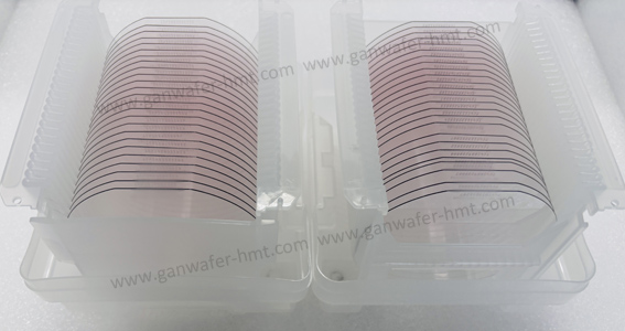
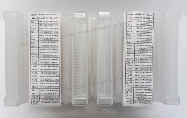
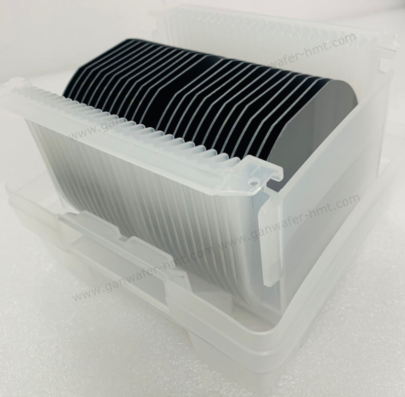
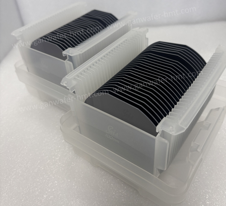
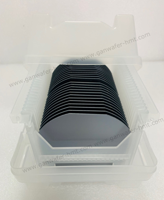
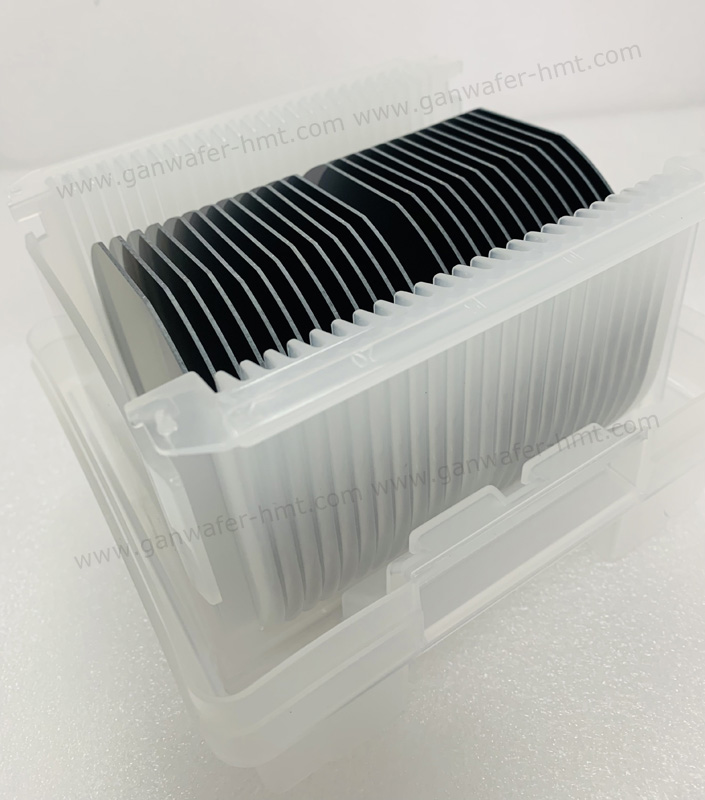
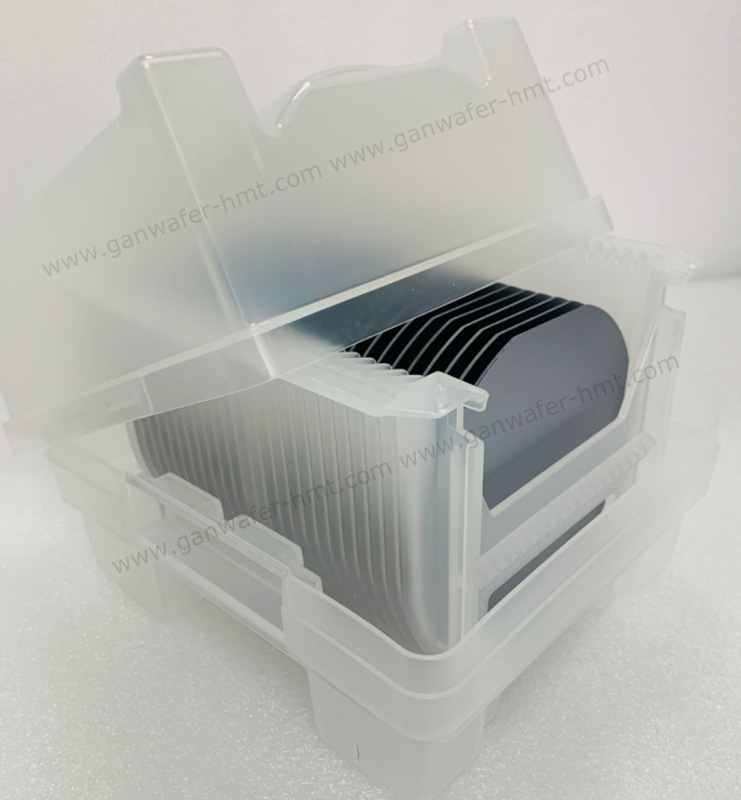
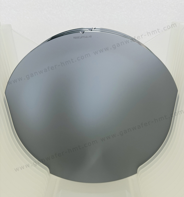
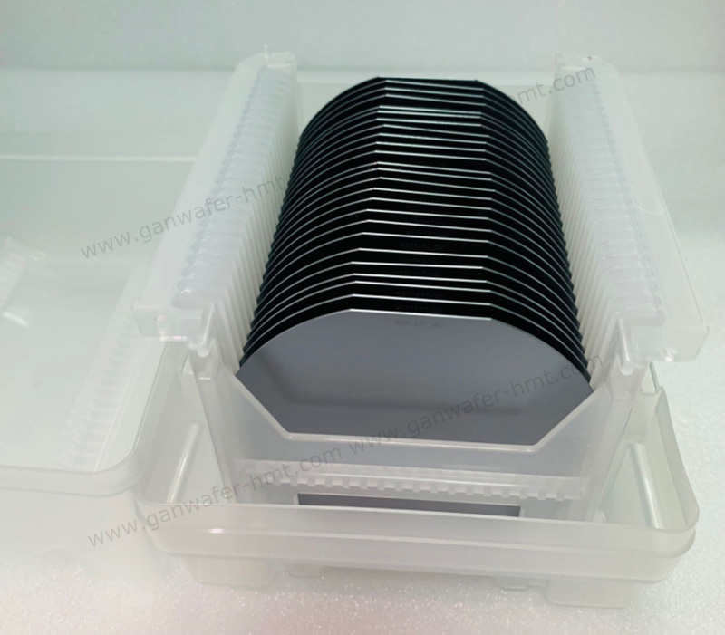
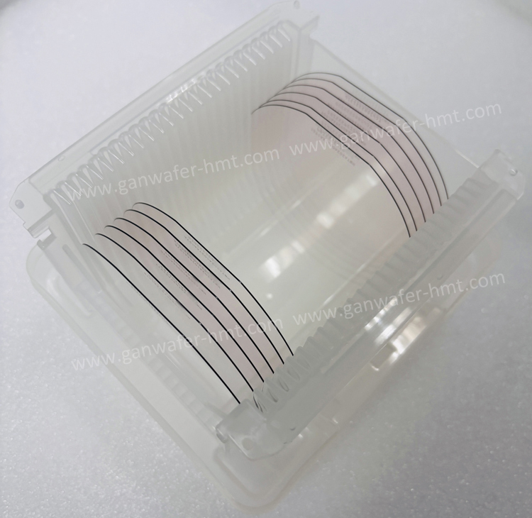
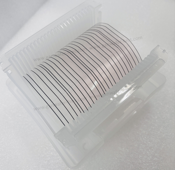
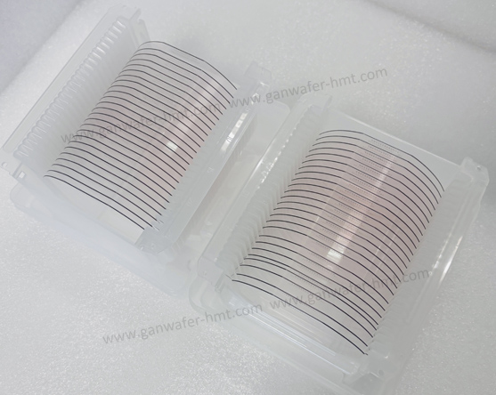
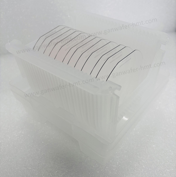
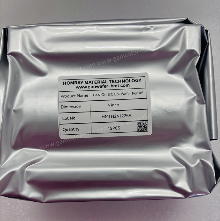
Substrate Size: 4 inch,6 inch
Substrate Thickness: 500um
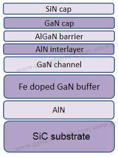
Cap Layer: SiN,GaN,pGaN
Product Description
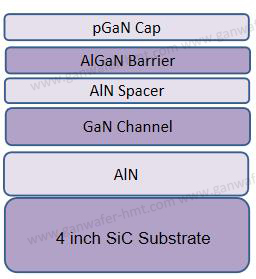
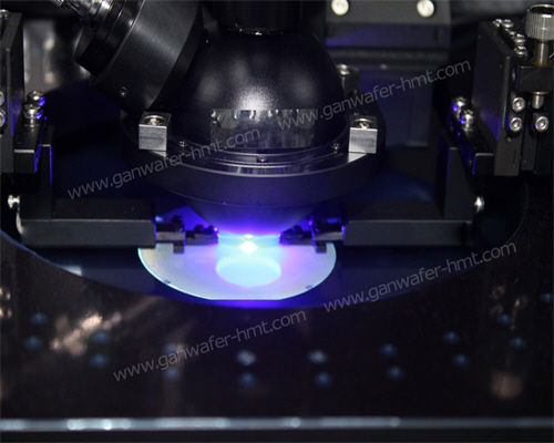
HMT, a leading professional GaN epi wafer manufacturer based in China, specializes in the production of high-quality GaN-on-SiC epi wafers. We offer a comprehensive range of wafer sizes including 4inch, 6inch, and 8inch diameters. Our product portfolio covers D-Mode, E-Mode, and RF structures to meet diverse application needs. All epi wafers are grown on premium 4H semi-insulating (4H-SI) SiC substrates, ensuring superior performance and reliability for advanced semiconductor applications.
GaN epitaxy has evolved from simple material growth into a systematic engineering project integrating structural design, defect control, doping processes, device integration, and industrial-scale manufacturing. Its applications in 5G communication, automotive radar, micro-displays, and high-frequency power supplies continue to expand.
GaN-on-SiC offers a relatively close lattice match (mismatch ~3.5%) and high thermal conductivity (significantly higher than sapphire or silicon), which facilitates heat dissipation in high-power, RF, and high-temperature devices. Its good electrical conductivity allows for backside electrode fabrication, making it suitable for high-frequency/high-voltage applications. However, SiC substrates are very hard and difficult to polish, and they typically have a higher threading dislocation density, with some defects potentially propagating into the GaN layer.
Our company typically introduces a high-quality AlN buffer layer before GaN growth to effectively reduce interface defects. We also enhance substrate surface treatment by improving polishing and cleaning processes. Currently, 4- to 6-inch wafers dominate the market, while 8-inch wafers represent the future mainstream, ideal for high-end applications such as RF power amplifiers (PAs), microwave systems, 5G base stations, and radar.
Related Products
![]() M.P: +86-15366208370 ; +86-15366203573
M.P: +86-15366208370 ; +86-15366203573
![]() E-mail: kim@homray-material.com;tina@homray-material.com
E-mail: kim@homray-material.com;tina@homray-material.com
HMT Silicon Carbide (SiC) Wafer Website: www.sicwafer-hmt.com