
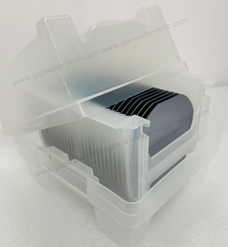
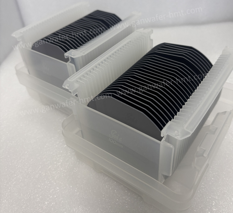
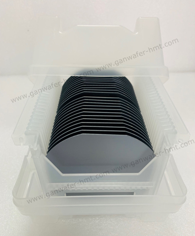
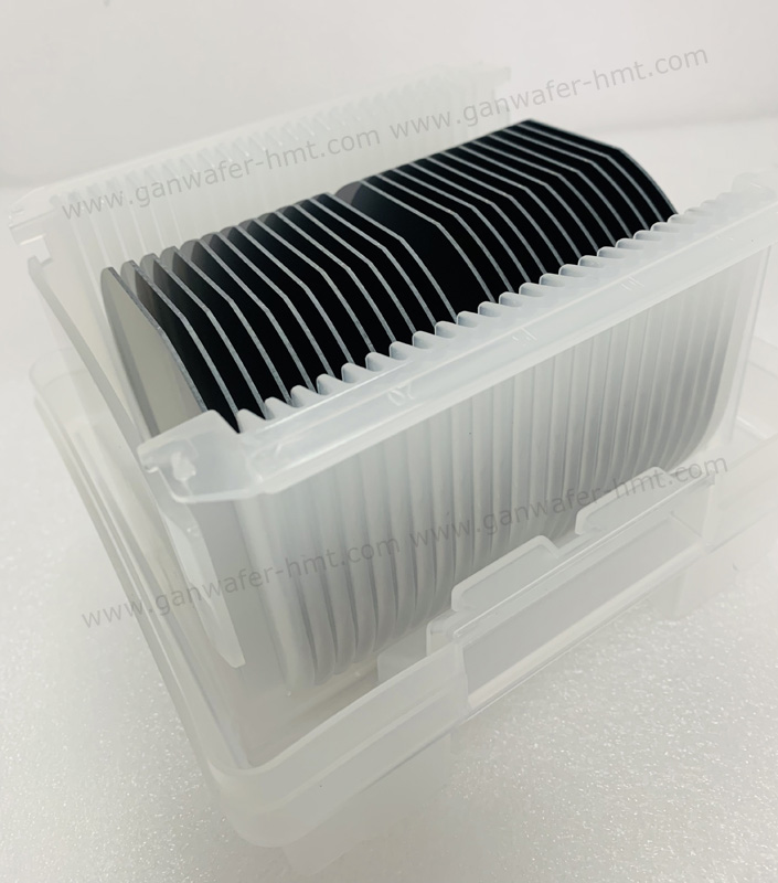
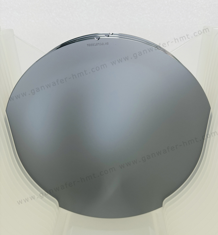
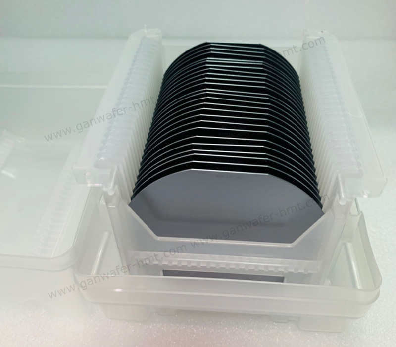
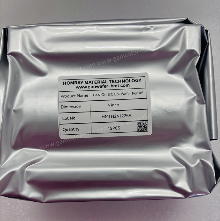
6inch GaN Epitaxial Wafer(AlGaN/SiN)
GaN-On-Si Epitaxial Wafer
Substrate Diameter:6 inch
Substrate Thickness:1000um
Cap Layer: SiN/GaN
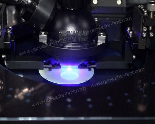
Product Description
Gallium nitride (GaN) is an inorganic compound with the chemical formula GaN. As a key semiconductor material, its high-quality production by GaN Epitaxial Wafer Manufacturers, such as in the form of 6 inch GaN on Si Epi Wafer, enables advanced applications. We produce D-HEMT structure and E-HEMT structure for different customers. It is a compound of nitrogen and gallium, typically appearing as a white or light-yellow solid powder. It exhibits characteristics such as structural stability, high melting point, high voltage resistance, and high hardness, making it suitable for extreme environments.
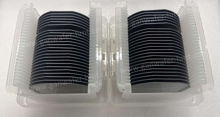
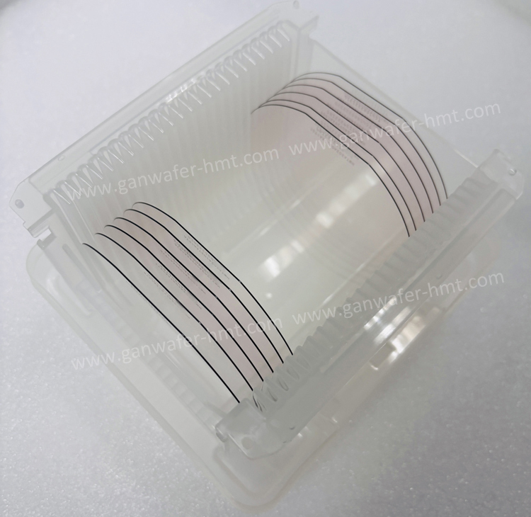
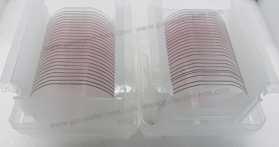
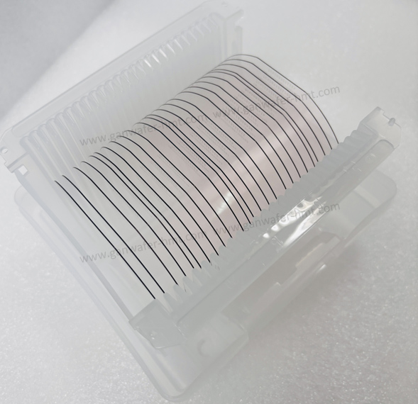
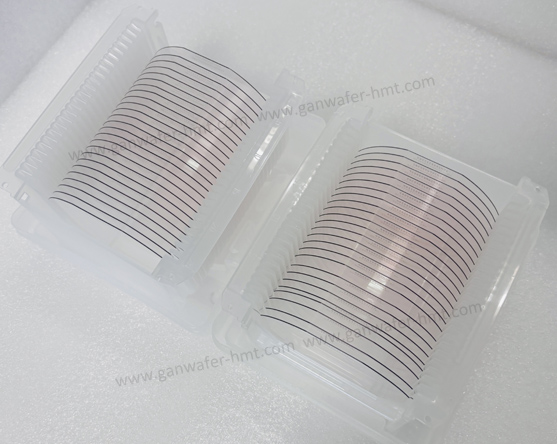
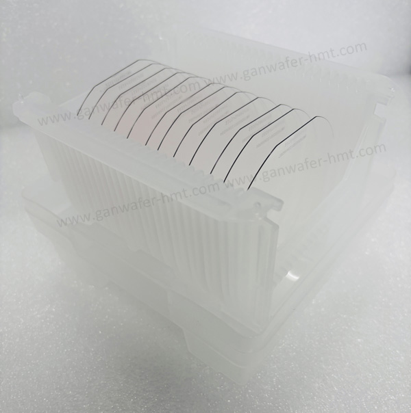
HMT GaN Epi Wafer
- Type: GaN on Si
- Structure: D-Mode, E-Mode
- Dimension: 4inch 6inch and 8inch
- Si Substrate Thickness: 675um, 1000um
- Cap Layer Thickness: SiN/GaN 0-5nm
Third-generation semiconductors, due to their wider bandgap, higher breakdown electric field, higher thermal conductivity, higher electron saturation rate, and superior radiation resistance, are more suitable for manufacturing high-temperature, high-frequency, high-power, and radiation-resistant devices. They can be widely applied in high-voltage, high-frequency, high-temperature, and high-reliability fields, including radio frequency communication, radar, satellites, power management, automotive electronics, and industrial power electronics.
Main Application Scenarios of Gallium Nitride
The current primary application directions of gallium nitride materials can be categorized into: power electronics, radio frequency electronics, and optoelectronics.
- Power Electronics: The low-loss and high-frequency material properties of gallium nitride give it significant advantages in power electronics, particularly in consumer electronics chargers and power adapters, where it holds considerable penetration potential. Low conduction loss: GaN has a bandgap three times wider than that of silicon and a breakdown electric field ten times higher. Under the same rated voltage, the on-resistance of GaN switching power devices is three orders of magnitude lower than that of silicon devices, significantly reducing conduction losses. High switching frequency: GaN devices can achieve switching frequencies exceeding 150 kHz in PFC applications and over 1 MHz in DC power converters, substantially reducing the size of magnetic components and enabling higher power density at lower costs.
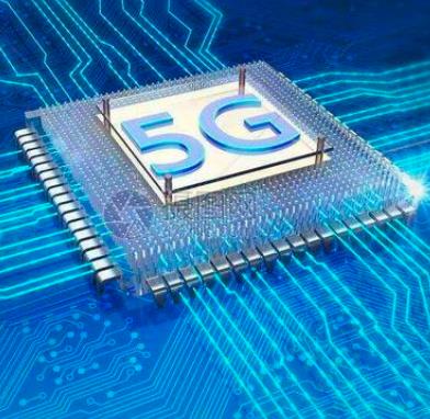
- Radio Frequency Electronics: Gallium nitride RF devices are primarily used in military radar, satellite communications, and 5G base stations. Due to national security concerns, overseas companies impose export restrictions on high-performance GaN devices to China. Driven by the urgent need for domestic alternatives, relevant GaN RF device companies have gradually broken foreign monopolies and achieved technological advancements.
- Optoelectronics: Compared to traditional silicon materials, gallium nitride offers higher electron mobility, a wider bandgap, better thermal conductivity, and greater toughness. These properties make gallium nitride highly advantageous in optoelectronics. Gallium nitride materials can be used to fabricate high-performance LEDs (light-emitting diodes) and LDs (laser diodes). LEDs, known for their high brightness, low power consumption, long lifespan, and environmental friendliness, are widely used in indoor and outdoor lighting, automotive lights, displays, and signal lights. LDs, on the other hand, are employed in communications, healthcare, and industrial processing due to their high energy conversion efficiency, compact size, and fast switching speed. Additionally, gallium nitride materials can be used to produce high-performance optoelectronic devices such as photodetectors, solar cells, and optical communication devices.
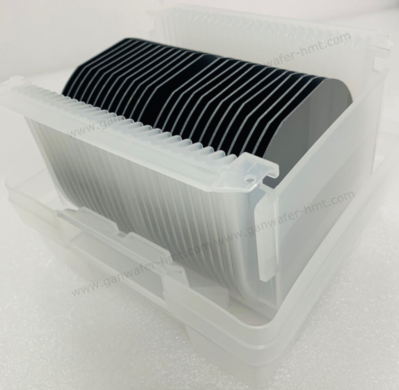
Related Products
![]() M.P: +86-15366208370 ; +86-15366203573
M.P: +86-15366208370 ; +86-15366203573
![]() E-mail: kim@homray-material.com;tina@homray-material.com
E-mail: kim@homray-material.com;tina@homray-material.com
HMT Silicon Carbide (SiC) Wafer Website: www.sicwafer-hmt.com