
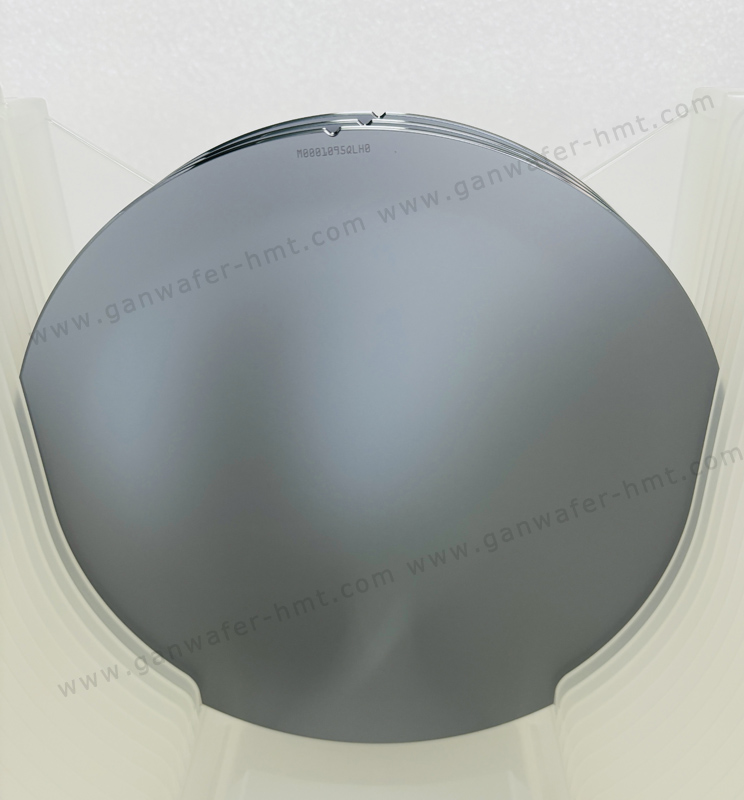
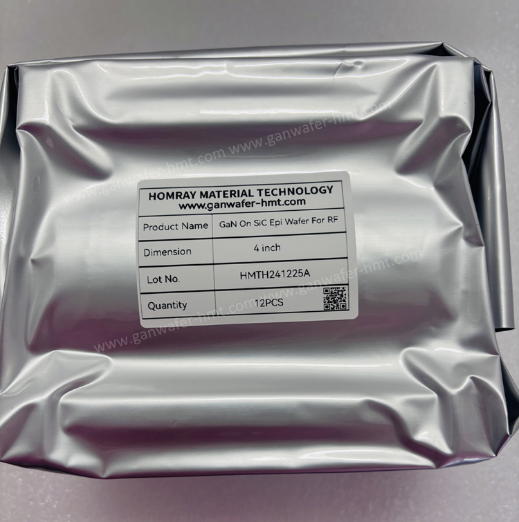
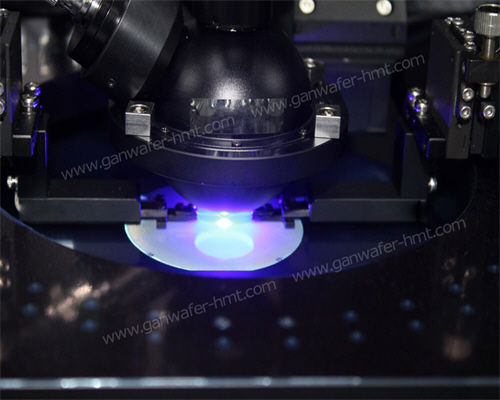
4'' GaN-On-SiC Epi Wafer For Power HEMT
GaN-On-SiC Epi Wafer
Substrate Size: 4 inch,6 inch
Substrate Thickness: 500um
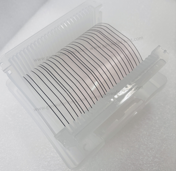
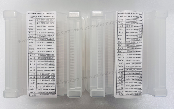
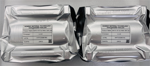
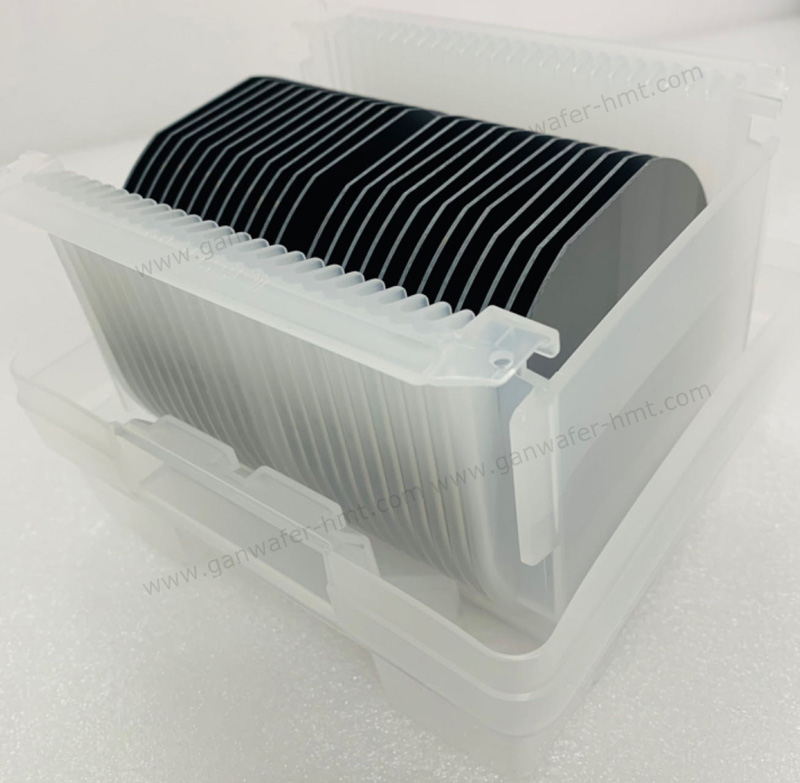
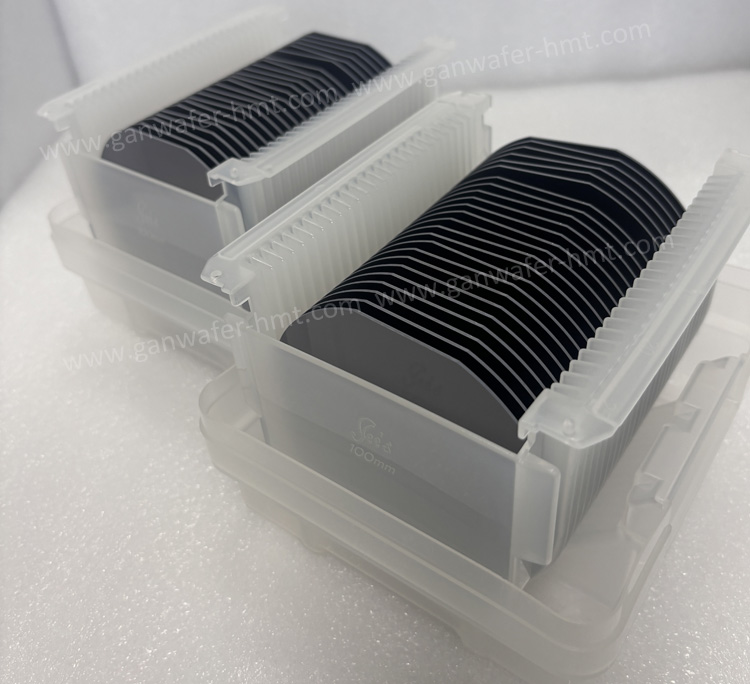
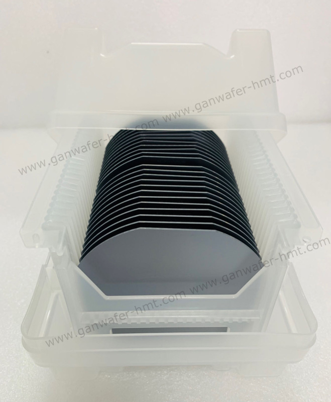
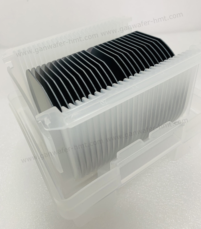
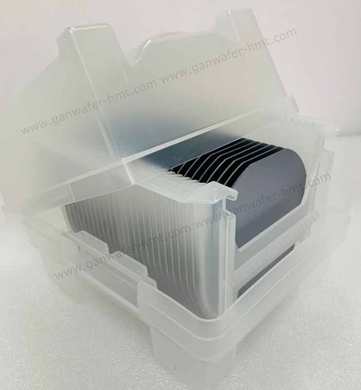
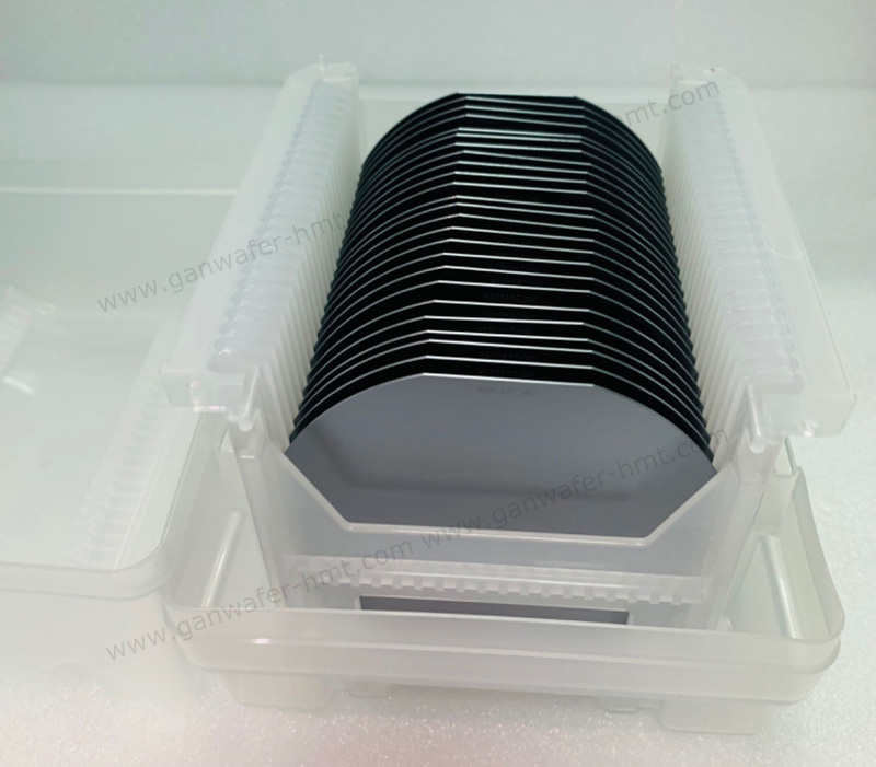
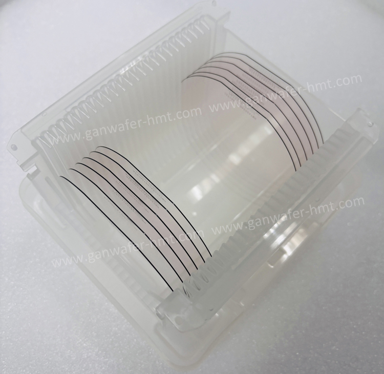
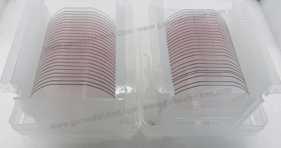
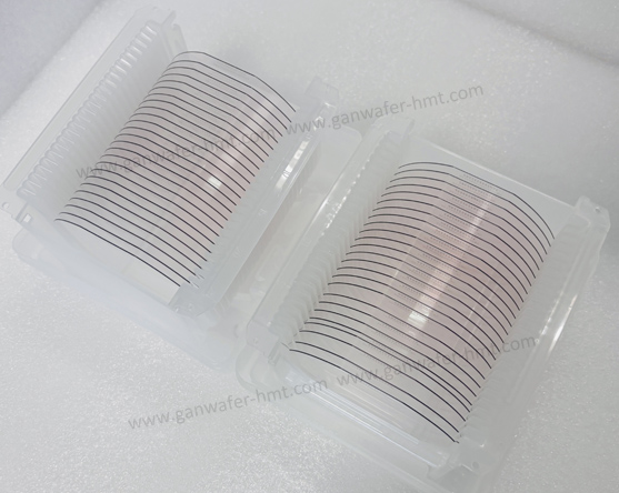
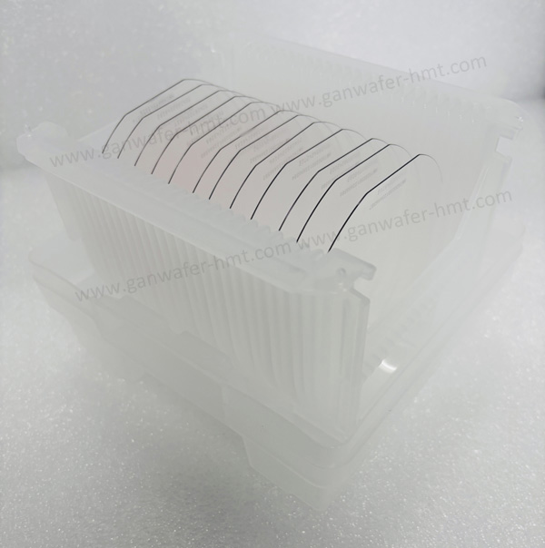
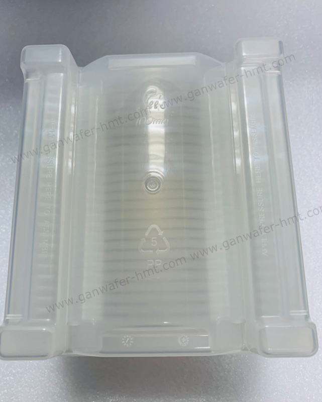
Package: Wafer Cassette
Product Description
Global GaN Epi Wafer Manufacturers HMT can offer 4'' GaN-on-SiC Epi Wafer for Power HEMT applications. We have 4inch,6inch and 8inch D-Mode and E-Mode two types. We use semi-insulating(resistivity ≥1E7ohm.cm ) SiC Wafer as the substrate, thickness 500±25um and growing by MOCVD. We support customize GaN Epi Wafer each layer thickness and cap layer type(GaN cap,SiN cap or p-GaN). Contact us and disscussing your GaN project now!
4 Inch GaN on SiC Epi Wafer Package
The close lattice constant match (mismatch of approximately 3.5%) and high thermal conductivity (significantly higher than sapphire/silicon) contribute to efficient heat dissipation in high-power, radio frequency, and high-temperature devices.
Excellent electrical conductivity allows for the fabrication of backside electrodes, making it suitable for high-frequency and high-voltage applications.
SiC exhibits superior thermal conductivity (three to four times that of silicon), enabling GaN-on-SiC devices to handle higher power densities while maintaining thermal stability. This directly translates to higher reliability, longer device lifespan, and the ability to reduce the overall size of amplifiers or integrate more power within a given form factor. Furthermore, the closer lattice match between silicon carbide and gallium nitride compared to silicon helps reduce dislocation defects during manufacturing and enables the development of more robust high-voltage devices.
Related Products
![]() M.P: +86-15366208370 ; +86-15366203573
M.P: +86-15366208370 ; +86-15366203573
![]() E-mail: kim@homray-material.com;tina@homray-material.com
E-mail: kim@homray-material.com;tina@homray-material.com
HMT Silicon Carbide (SiC) Wafer Website: www.sicwafer-hmt.com