
6''8'' SiC Wafer Suppliers For AR AI
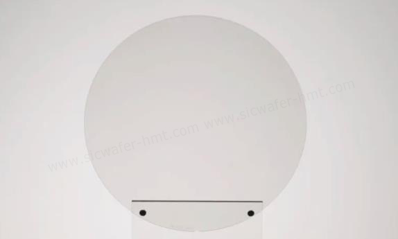
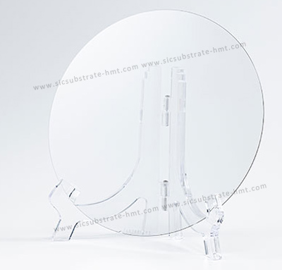
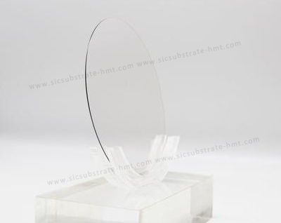
Diameter: 150mm /200mm
Grade: Production
Thickness: 500±25um
Type: HPSI
Product Description
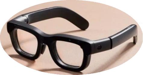
As a premier Silicon Carbide (SiC) wafer suppliers, our advanced 6 inch and 8 inch semi-insulating SiC wafers are engineered specifically for high-frequency optoelectronic applications. We provide the essential substrate foundation for the next generation of Augmented Reality(AR) and AI glasses. With exceptional thermal conductivity, superior hardness, and excellent optical properties, our wafers enable the development of smaller, more powerful, and more efficient waveguides and micro-displays. This ensures AR glasses deliver crisp, vibrant visuals and seamless AI processing, setting a new standard for performance and reliability in wearable optics.
Semi-insulating SiC Wafer Spec
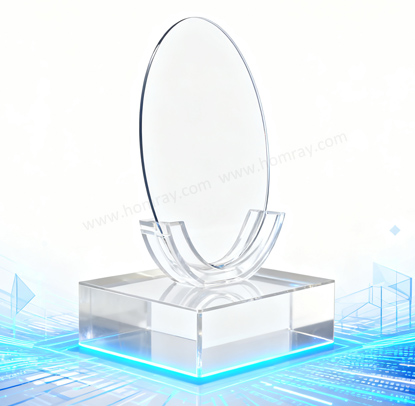
- Diameter: 150±0.2 mm or 200±0.2 mm
- Grade: Production
- Thickness: 500±25 um
- Surface Orientation:{0001}±0.5°
- Refractive Index:>2.65@589nm
- Absorption: <0.5%@450-650nm
- Haze: <0.3%@visible
- Notch orientation: <1-100>±1°
- Notch Depth: 1~1.25mm
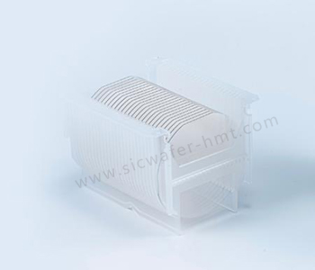
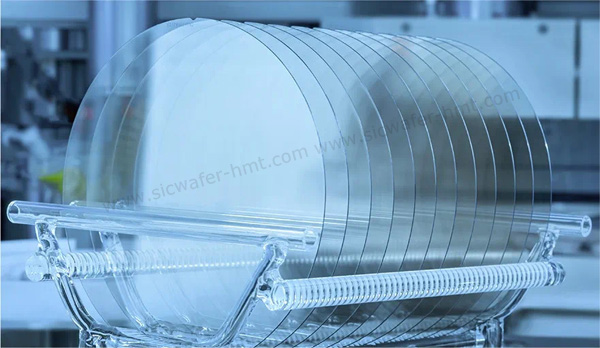
- Surface : Double side CMP
Key Features of HPSI SiC Wafers for AR Glasses
- The high refractive index of SiC wafers(2.7) enables a single-layer lens to achieve a full-color field of view exceeding 80°, while resolving the common "rainbow artifact" issue in AR glasses. In contrast, traditional glass lenses require stacking three layers to reach only 40°. SiC material can thus provide a longer eye relief, larger field of view, and clearer visual experience.
- The high refractive index of SiC also allows the three color channels (red, green, and blue) to be combined into a single-piece waveguide. This differs from current waveguide designs that typically use two or three separate glass pieces—each dedicated to one color (or one piece for two colors). Adopting SiC material can improve the size, weight, and cost of AR glasses.
- The high thermal conductivity of SiC enhances the thermal management of AR glasses. It not only rapidly draws heat away from the optical engine to prevent thermal accumulation that causes optical performance degradation (such as rainbow patterns and color shift) but also allows for wafer-level microstructural design to shorten heat transfer paths. By integrating material R&D and optical processing capabilities, the mass production of low-cost, high-performance AR lenses will be accelerated.
Related Products


![]() M.P: +86-15366208370 ; +86-15366203573
M.P: +86-15366208370 ; +86-15366203573
![]() E-mail: kim@homray-material.com;tina@homray-material.com
E-mail: kim@homray-material.com;tina@homray-material.com
HMT Silicon Carbide (SiC) Wafer Website: www.sicwafer-hmt.com