

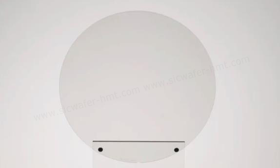
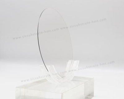
HPSI SiC Wafer Manufacturers for RF and GaN-on-SiC
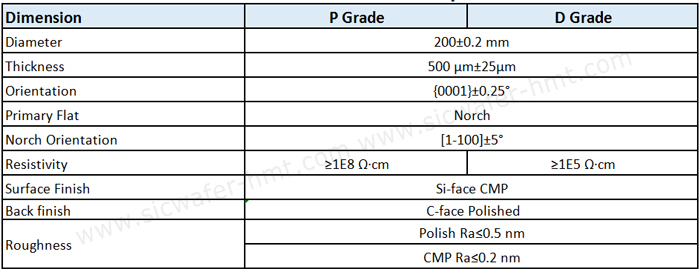
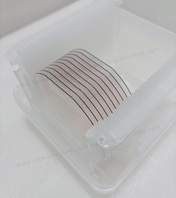
Diameter: 200±0.2mm
Grade: D/P
Thickness: 500±25um
Type: HPSI
Product Description
HPSI SiC Wafer Manufacturers for Advanced RF Semiconductor Applications
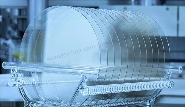
HMT is a professional manufacturer of High Purity Semi Insulating (HPSI) SiC Wafers designed for high-frequency semiconductor applications, including RF devices, microwave electronics and GaN-on-SiC technologies. Unlike conductive SiC substrates mainly used for power electronics, HPSI SiC wafers provide extremely high electrical resistivity and excellent thermal conductivity, making them an ideal platform for advanced RF and communication semiconductor devices.
Our 4inch 6inch and 8inch HPSI SiC substrates combine superior crystal quality, low defect density and stable electrical properties to support demanding semiconductor fabrication processes.
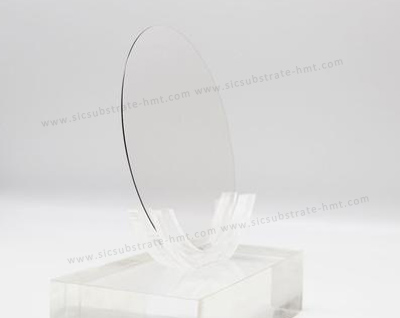
What Is an HPSI SiC Wafer?
A High Purity Semi Insulating SiC Wafer (HPSI SiC Wafer) is a silicon carbide substrate with high resistivity characteristics achieved through advanced crystal growth and material control technologies. HPSI SiC substrates are widely used when electrical isolation and excellent thermal performance are required.
Compared with conductive SiC wafers, HPSI SiC wafers are optimized for:
* RF power devices
* Microwave circuits
* GaN epitaxial growth
* High-frequency communication systems
Key Advantages of HPSI SiC Substrate
Excellent Electrical Isolation
High resistivity characteristics reduce parasitic effects and improve device performance in high-frequency applications.
Superior Thermal Management
SiC provides excellent thermal conductivity, allowing RF devices to operate under high power density conditions.
High Crystal Quality
Advanced manufacturing processes ensure:
- Low defect density
- Stable wafer performance
- Improved epitaxial compatibility
Ideal Platform for GaN-on-SiC Technology
HPSI SiC substrates are widely selected as the supporting material for GaN epitaxial layers because of their excellent thermal and electrical properties.
HPSI SiC Wafer Applications
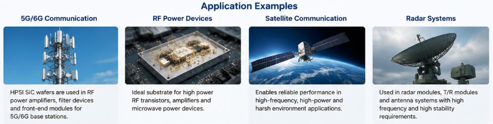
RF Power Devices
HPSI SiC wafers are used for:
※RF amplifiers
※Microwave devices
※Radar systems
※Communication infrastructure
GaN-on-SiC Semiconductor Technology
GaN-on-SiC combines the high-frequency capability of GaN with the thermal advantages of SiC.
Applications include:
※5G base stations
※Satellite communication
※Defense electronics
※High-power RF systems
High Frequency Electronics
HPSI SiC substrates support advanced semiconductor designs requiring:
※Low signal loss
※High thermal stability
※High operating frequency

What is the difference between HPSI SiC and conductive SiC wafer?
Conductive SiC wafers are mainly used for power devices such as MOSFETs, while HPSI SiC wafers are optimized for RF and high-frequency applications requiring electrical isolation.
Why is SiC used for GaN RF devices?
SiC provides excellent thermal conductivity and mechanical stability, making it an ideal substrate material for GaN RF semiconductor devices.
Related Products
 E-mail: kim@homray-material.com;tina@homray-material.com
HMT Silicon Carbide (SiC) Wafer Website: www.sicwafer-hmt.com