
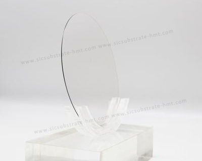
Optics SiC Wafer Manufacturer
Diameter: 200±0.2mm
Grade: Production
Thickness: 500±25um
Type: HPSI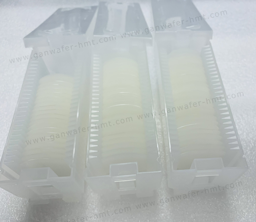
2 Inch GaN-On-Sapphire Template
Dimensions: Ф 50.8 mm ± 1 mm
Thickness:4.5µm, 20 µm
Orientation:C-plane(0001) ± 0.5°
Useable Surface Area:> 90%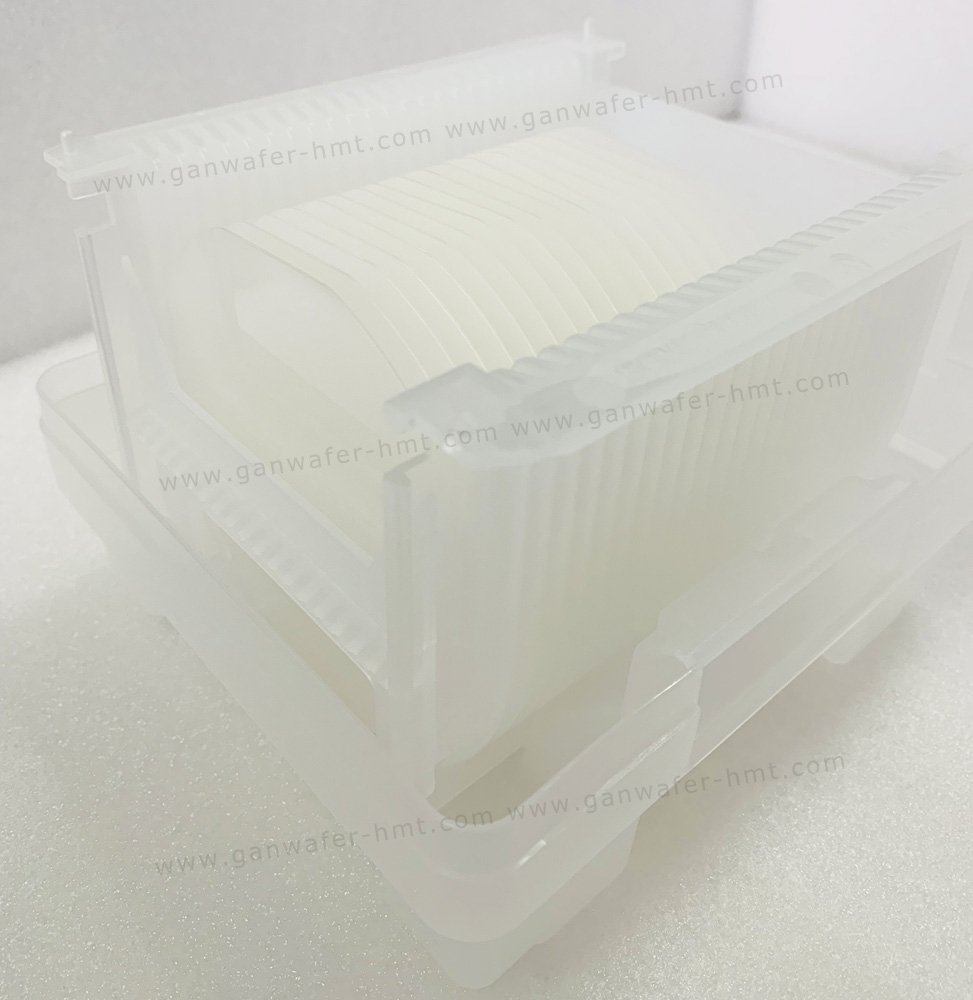
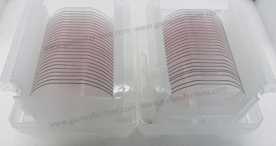
4 Inch GaN-On-Sapphire Template
Dimensions: Ф 100 mm ± 0.1 mm
Thickness:4.5 µm, 20 µm
Orientation:C-plane(0001) ± 0.5°
Useable Surface Area:> 90%
2 Inch Free-Standing GaN Substrate
Dimensions: Ф 50.8 mm ± 1 mm
Thickness: 350 ± 25 µm
Useable Surface Area: > 90%
Total Thickness Variation: ≤ 15 µm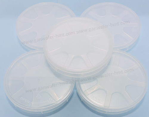
4 Inch Free-Standing GaN Substrate
Dimensions: Ф 100 mm ± 1 mm
Thickness: 400 ± 50 µm
Useable Surface Area: > 90%
Total Thickness Variation: ≤ 40 µm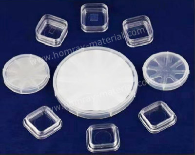
Square Free-Standing GaN Substrate
Dimension:10*15mm²
Thickness: 350±25um
Useable Surface Area:>90%
Conduction Type: N Type,SI Type
GaN Epitaxial On Si For RF HEMT
GaN-On-Si Epi Wafer For RF HEMT
Substrate Diameter:6 inch (111)
Substrate Thickness:1000um
Epi Layer Total Thickness: 1.5~2.0um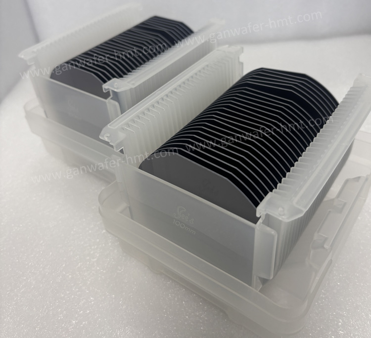
GaN Epitaxial On Si For Power HEMT
GaN-On-Si Epi Wafer For Power HEMT-D Mode
Substrate Diameter: 4-8 inch(111)
Substrate Thickness: 675,1000um
Epi Layer Total Thickness: 2~5.5um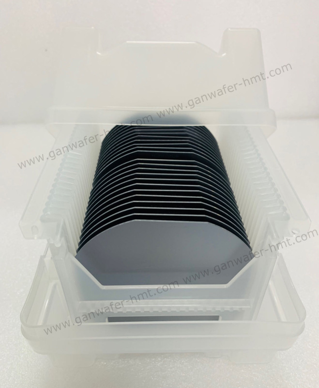
Gan Epitaxial On Si For Power HEMT E-Mode
GaN-On-Si Epi Wafer For Power HEMT-E Mode
Substrate Diameter: 4-8 inch(111)
Substrate Thickness: 675,1000um
Epi Layer Total Thickness: 2~5.5um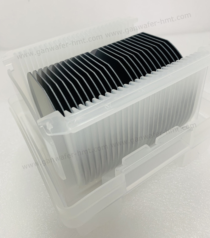
pGaN HEMT On Si Epi Wafer
GaN-On-Si Epi Wafer
Substrate Size: 4 inch,6 inch,8 inch
Substrate Thickness: 675um,1000um
GaN Buffer Layer: 2-3um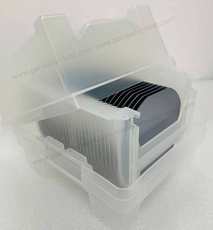
6inch GaN Epitaxial Wafer(AlGaN/SiN)
GaN-On-Si Epitaxial Wafer
Substrate Diameter:6 inch
Substrate Thickness:1000um
Cap Layer: SiN/GaN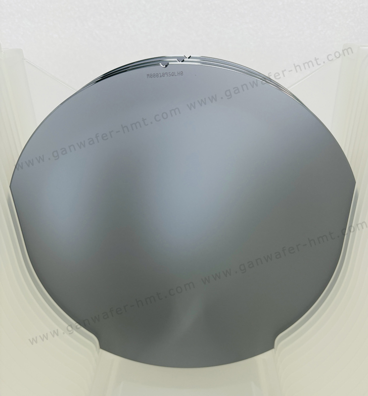
8 inch GaN-on-Si Epitaxial Wafer
GaN-On-Si Epi Wafer
Substrate Size: 8 inch
Substrate Thickness: 1000um
GaN Buffer Layer: 2-3um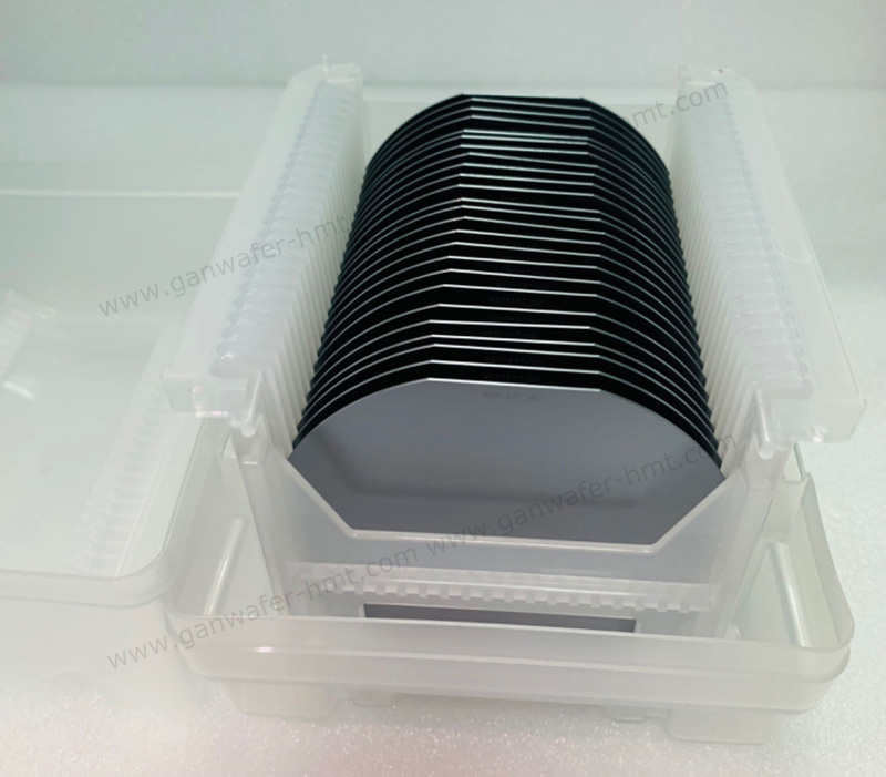
GaN Epi grown on Si wafer
GaN-On-Si Epi Wafer
Substrate Size: 4/6/8 inch
Substrate Thickness: 675um 1000um
GaN Buffer Layer: 2-3um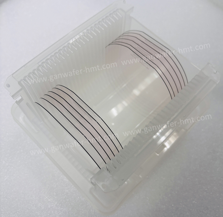
GaN Epitaxial On SiC For Power HEMT
GaN-On-SiC Epi Wafer For Power HEMT
Substrate Size: 4 inch,6 inch
Substrate Thickness: 500um
GaN Buffer Layer: 2-3um
GaN Epitaxial (Epi) Wafer Manufacturers
RF and Power HEMT
Substrate Size: 4 inch,6 inch
Substrate Thickness: 500um
Cap Layer: SiN,GaN,pGaN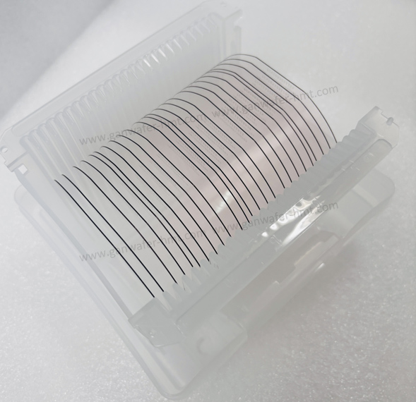
4'' GaN-On-SiC Epi Wafer For Power HEMT
GaN-On-SiC Epi Wafer
Substrate Size: 4 inch,6 inch
Substrate Thickness: 500um
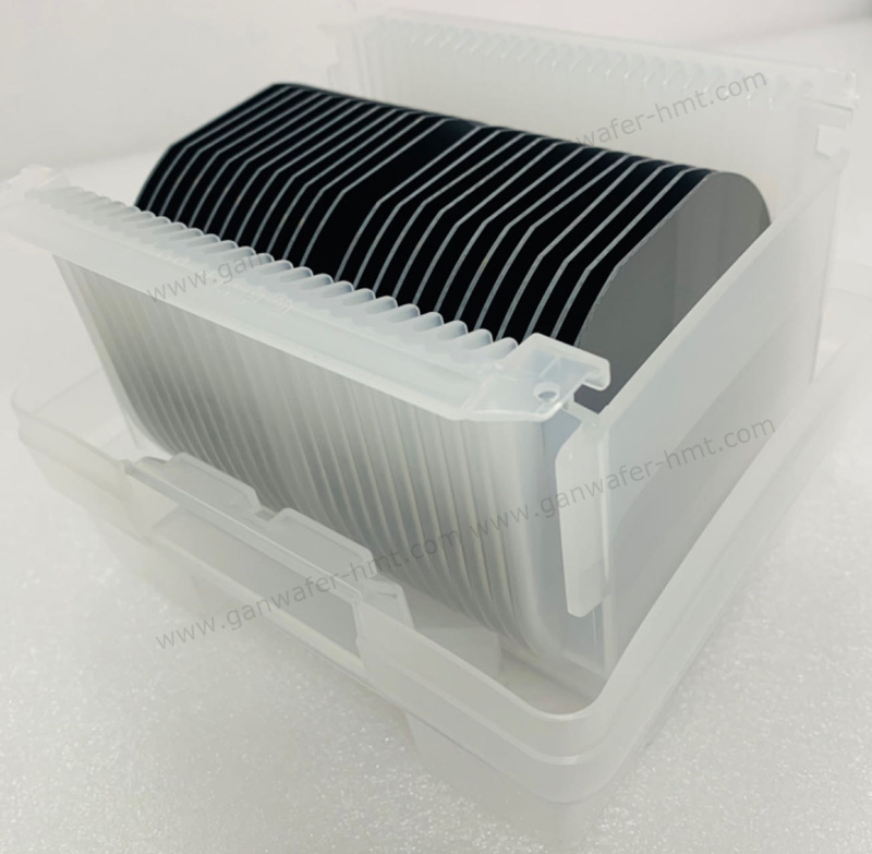
Package: Wafer Cassette
![]() E-mail: kim@homray-material.com;tina@homray-material.com
E-mail: kim@homray-material.com;tina@homray-material.com
HMT Silicon Carbide (SiC) Wafer Website: www.sicwafer-hmt.com