
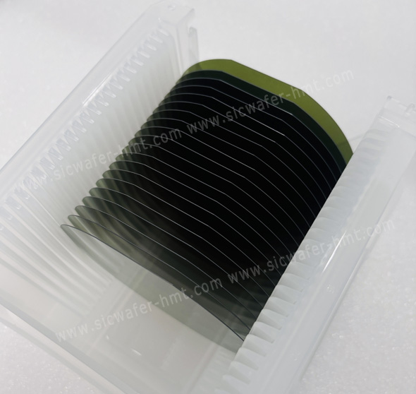
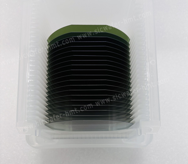
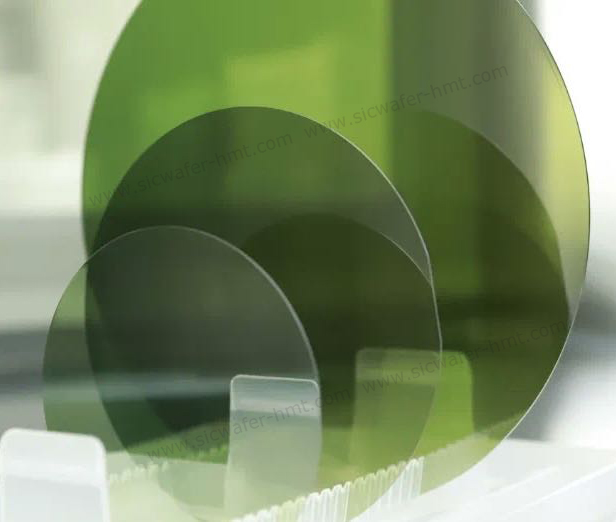
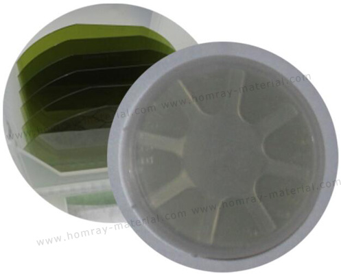
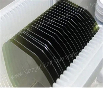
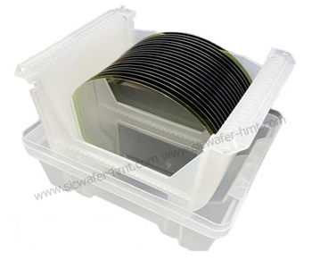
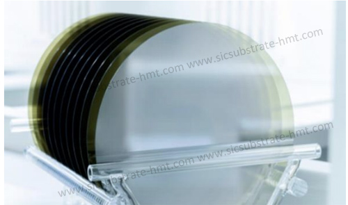
DSP 4-inch SiC Substrate Manufacturer
Diameter: 100±0.2mm
Grade: R Grade,P Grade
Thickness: 350±25um
Type: Conductive N
Product Description
Silicon carbide (SiC) is a core representative of third-generation semiconductor materials, widely adopted by 4 inch SiC substrate manufacturers who produce wafers with key specifications such as thickness of 350um, micro-pipe density (MPD) <0.2 cm⁻², and total thickness variation (TTV) <10um. These high-quality SiC substrates enable the material’s excellent physical properties—including wide bandgap, high breakdown electric field strength, and high thermal conductivity—making SiC an ideal choice for high-voltage, high-temperature, and high-frequency applications.
Key Physical Property Comparison:
-
Bandgap: Approximately 3.26 eV, three times that of silicon (Si), resulting in extremely low leakage current and higher temperature tolerance.
-
Breakdown Field Strength: Approximately 3-4 MV/cm, 10 times that of silicon, meaning the drift layer of devices can be made thinner at the same voltage, significantly reducing on-state resistance.
-
Thermal Conductivity: Approximately 4.9 W/(cm·K), three times that of silicon and even higher than copper, offering excellent heat dissipation and making it highly suitable for high-power-density devices.
- Electron Saturation Drift Velocity: Twice that of silicon, making it suitable for high-frequency switching applications.
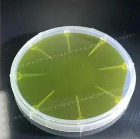
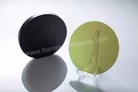
Conductive SiC Substrate (N-type):
-
Low resistivity (15-30 mΩ·cm), used for manufacturing power devices (MOSFETs, diodes), with downstream applications in new energy vehicles, photovoltaics, energy storage, etc.
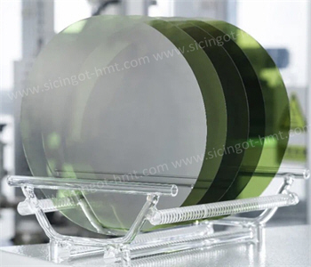
Semi-insulating SiC Substrate:
-
Very high resistivity (>10^5 Ω·cm), used for manufacturing RF devices (HEMT), with downstream applications in 5G communications, radar, etc.; the latest trend is its use in AR glasses for optical waveguide lenses.
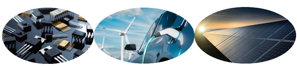
Downstream Applications (Three Major Drivers):
-
Traditional Core: New energy vehicles (main drive, OBC, DC-DC), photovoltaics and energy storage, charging piles.
-
Emerging Stars: AI server power supplies (PSUs), advanced packaging heat dissipation (CoWoS Interposer), AR glasses.
Related Products
![]() E-mail: kim@homray-material.com;tina@homray-material.com
E-mail: kim@homray-material.com;tina@homray-material.com
HMT Silicon Carbide (SiC) Wafer Website: www.sicwafer-hmt.com