
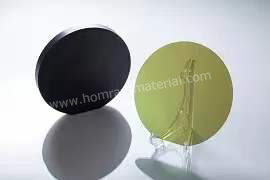
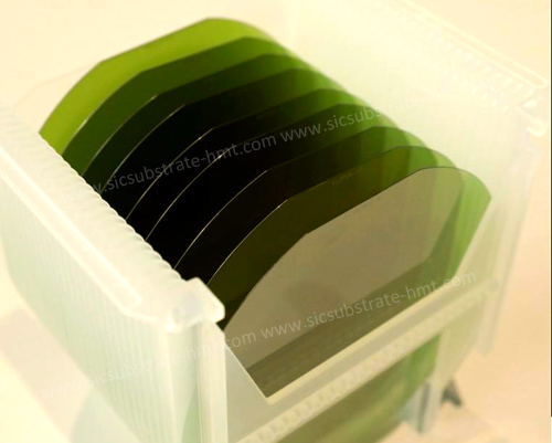
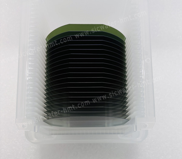
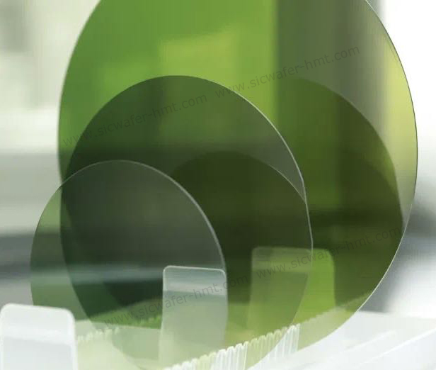
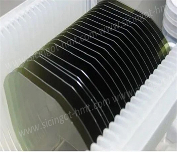
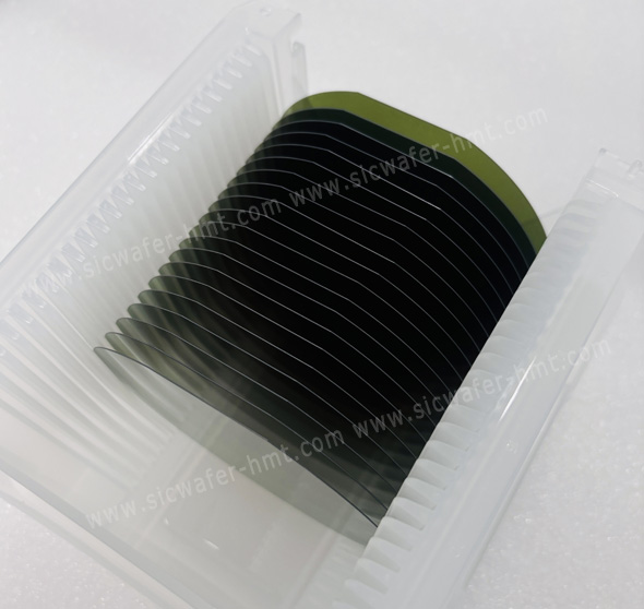
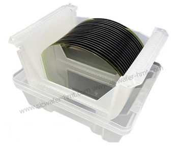
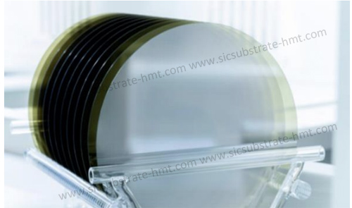
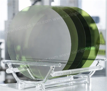
4'' SiC Wafer 100mm Diameter Producer
Diameter: 100±0.2mm
Grade: Research/Production
Thickness: 350um
Type: Conductive N
Product Description
Quality is the cornerstone of our operation as a professional SiC Wafer Manufacturer. We produce 4" SiC Wafer(100mm Diameter) with conductive type (resistivity 0.015-0.025ohm.cm). HMT can support customize various thickness SiC Wafer with the best price. We utilize advanced crystal growth techniques to produce substrates with exceptionally low micro-pipe density (<0.2 cm⁻²) and superior surface roughness. This commitment to material perfection provides our customers with the foundation needed to achieve high yields and superior performance in their SiC epitaxy and device fabrication processes.
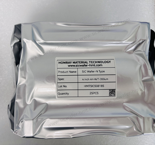
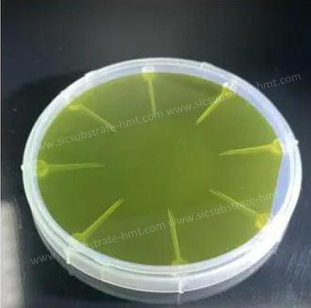
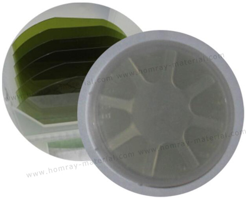
100mm 4inch SiC Wafer Package
Third-generation semiconductors exhibit excellent voltage resistance, making them ideal materials for high-power devices. The primary materials in this category are silicon carbide (SiC) and gallium nitride (GaN). SiC has a bandgap of 3.2 eV, while GaN has a bandgap of 3.4 eV—both significantly wider than silicon’s bandgap of 1.12 eV. Due to their inherently wide bandgaps, third-generation semiconductors demonstrate superior voltage and thermal tolerance, making them well-suited for high-power applications. Among them, silicon carbide has gradually entered large-scale adoption, with SiC diodes and MOSFETs already commercialized in the power device market.
Conductive substrates are widely used in power devices, with downstream applications including:
- new energy vehicles
- photovoltaics
- high-speed rail
- industrial power supplies
Conductive SiC substrates are primarily employed in the fabrication of power devices, which serve as critical fundamental components in the power electronics industry. These devices are extensively used in electric power conversion and circuit control across various types of power equipment, impacting a wide range of economic and daily life applications.
Related Products
![]() E-mail: kim@homray-material.com;tina@homray-material.com
E-mail: kim@homray-material.com;tina@homray-material.com
HMT Silicon Carbide (SiC) Wafer Website: www.sicwafer-hmt.com