
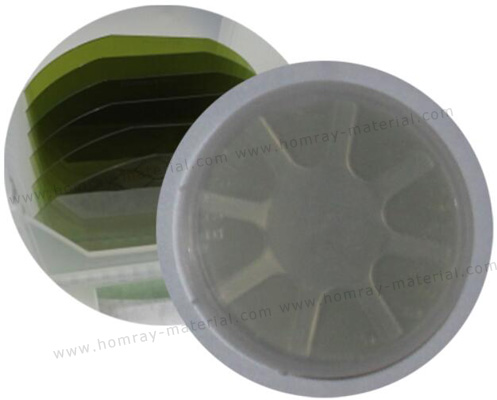
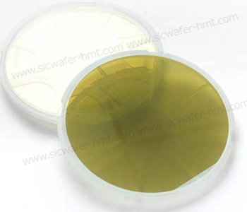
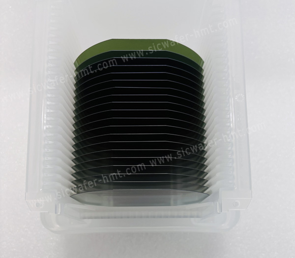
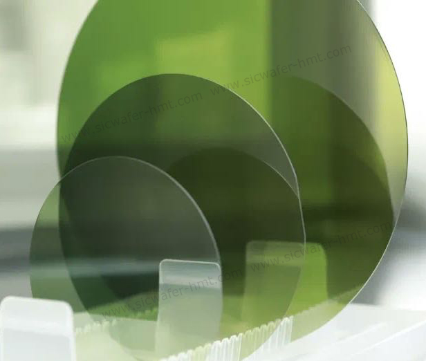
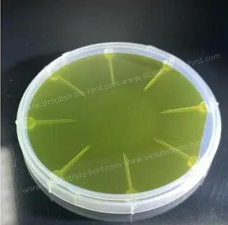
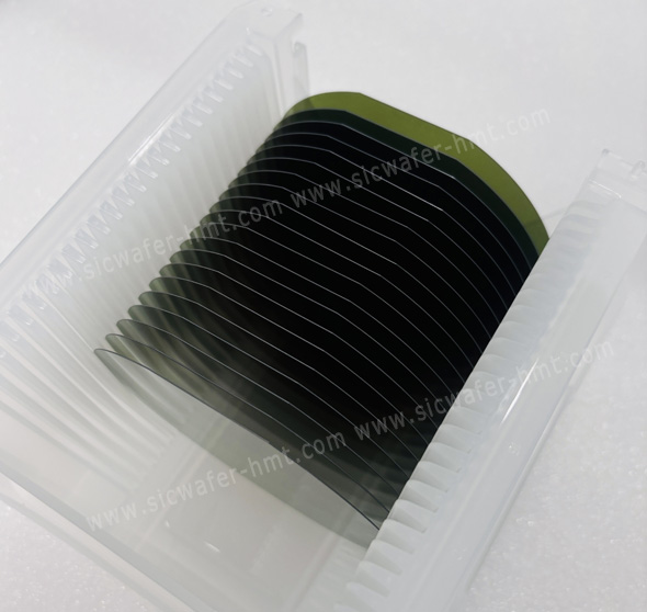
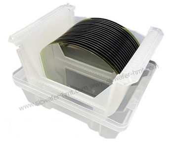
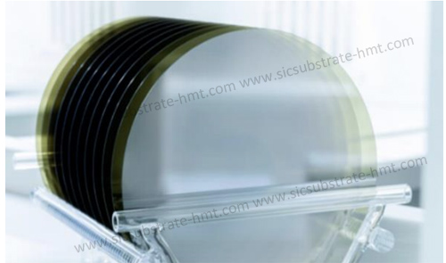
4" SiC Wafer N Type Manufacturer
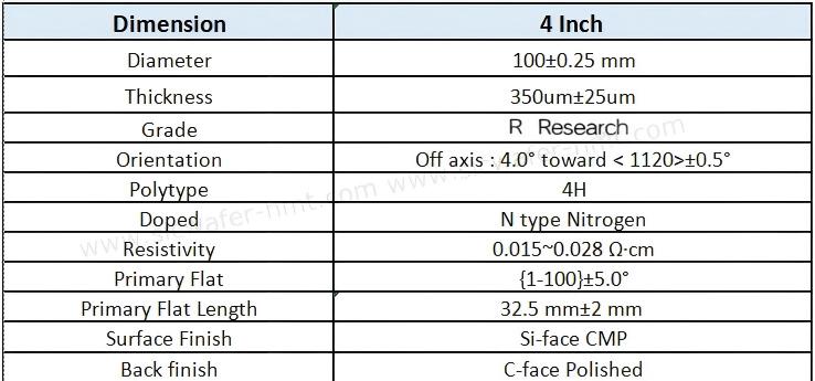
Diameter: 100±0.2mm
Grade: Research
Thickness: 350±25um
Type: Conductive N
Product Description
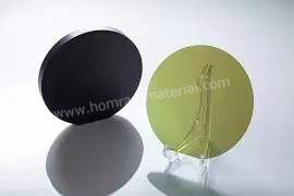
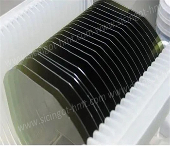
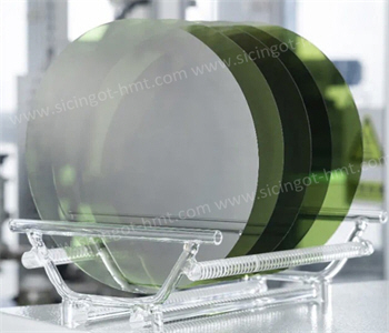
Leading SiC Wafer Manufacturer and Maker-HMT can still produce 4inch(100mm) SiC Wafer Research grade. As you know, the largest dimension of SiC wafer is 12inch now and mainstream is 6inch and 8inch. They stopped production 4'' anymore, but in HMT we still keep few capacity allocation for some customers which only need 4'' Silicon Carbide wafers. Meanwhile, we also have 4 inch P grade SiC Wafer for mass production.
100mm SiC Wafer Basic Parameters
Silicon Carbide Wafer Characteristics
The unique electronic band structure of silicon carbide (SiC) wafers is the key to their superior performance. The wide bandgap creates a high barrier for electrons to overcome, resulting in two critical advantages:
High-Temperature Stability: Low intrinsic carrier concentration enables SiC devices to operate at elevated temperatures without significant leakage current, making them ideal for harsh environments.
High Breakdown Electric Field: The wide bandgap also enhances the ability to withstand high voltages, resulting in high blocking voltage and low on-resistance.
Beyond electrical properties, SiC wafers also excel in thermal and mechanical performance:
Efficient Heat Dissipation: Exceptional thermal conductivity allows SiC to dissipate heat effectively—a crucial feature for high-power applications.
Durability in Harsh Environments: High mechanical strength and hardness make SiC resistant to wear and tear, suitable for demanding conditions.
Beyond electrical properties, SiC wafers also excel in thermal and mechanical performance:
Efficient Heat Dissipation: Exceptional thermal conductivity allows SiC to dissipate heat effectively—a crucial feature for high-power applications.
Related Products
![]() E-mail: kim@homray-material.com;tina@homray-material.com
E-mail: kim@homray-material.com;tina@homray-material.com
HMT Silicon Carbide (SiC) Wafer Website: www.sicwafer-hmt.com